


Bus Controller (BC)
8-13
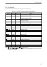
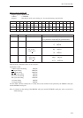
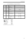
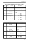
When using DRAM (Memory control register 1B B1DRAM = 1)
Bit No. Bit name Description Setting conditions
0 DRAM Block 1 DRAM 1: Use as DRAM space.
space setting
2 BM Block 1 bus mode 1: Asynchronous mode (MCLK synchronization)
3 PE Block 1 software page 0: Disabled
mode enable 1: Enabled
4 BW Block 1 bus width 0: 8 bits
1: 16 bits
7 to 6 ASA1 to 0 Always set to "01". Any setting other than "01" is prohibited.
10 to 8 ASN2 to 0 RAS precharge cycle 000: prohibited
(use as RP parameter) 001: 1MCLK
111: 7MCLK
15 to 11 WEN4 to 0 WE negate timing Settings other than those shown below are prohibited.
Set so that: 00100: 4MCLK
CAO (ADE)+CAS (REN)
≥ WEN 11111: 31MCLK
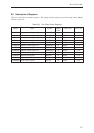
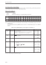
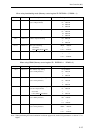
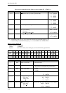
After the reset is released, block 1 is set as follows:
Address output end timing 3MCLK
RE negate timing 29MCLK
WE negate timing 29MCLK
RE/WE assert timing 3MCLK
Bus cycle start timing 0MCLK
Bus cycle end timing 31MCLK
AS assert timing 1MCLK
AS negate timing 3MCLK
The bus width is 16 bits, and synchronous mode is set.
~
~
~
~