


Bus Controller (BC)
8-19
8.6.4 Memory Block 3 Control Register
Memory control register 3A/B is used to set the memory block 3 read/write timing, synchronous/asynchronous
mode, fixed wait/handshaking mode, and bus width through software. However, the handshaking mode can only be
set when (MCLK frequency/SYSCLK frequency) = 4.
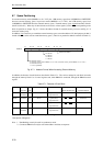
Memory control register 3A
Register symbol: MEMCTR3A
Address: x’32000036
Purpose: Sets the access timing, etc., for external memory space block 3.
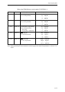
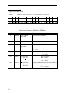
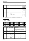
Bit No. 15 14 13 12 11 10 9876543210
Bit B3 B3 B3 B3 B3 B3 B3 B3 B3 B3 B3 B3 B3 B3 B3 B3
name REN4 REN3 REN2 REN1 REN0 BCE4 BCE3 BCE2 BCE1 BCE0 ADE1 ADE0 EA1 EA0 BCS1 BCS0
Reset 1 1 10111111111100
Access R/W R/W R/W R/W R/W R/W R/W R/W R/W R/W R/W R/W R/W R/W R/W R/W
Note: For the external memory access timing charts, refer to section 8.13, “External Memory Space Access (Non-
DRAM Spaces).”
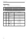
When using fixed wait mode (Memory control register 3B B3WM = 0)
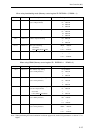
Bit No. Bit name Description Setting conditions
1 to 0 BCS1 to 0 Bus cycle start timing 00: 0MCLK
When nfr = 2, settings other than “00” or “01” are prohibited. 01: 1MCLK
When nfr = 1, settings other than “00” are prohibited. 10: 2MCLK
11: 3MCLK
3 to 2 EA1 to 0 RE/WE assert timing 00: 0MCLK
11: 3MCLK
5 to 4 ADE1 to 0 Address output end timing 00: 0MCLK
11: 3MCLK
10 to 6 BCE4 to 0 Bus cycle end timing Settings other than those
Set so that: shown below are prohibited.
BCE ≥ REN, BCE ≥ WEN ≥ EA 00100: 4MCLK
BCE ≥ASN + ADE
11111: 31MCLK
15 to 11 REN4 to 0 RE negate timing Settings other than those
shown below are prohibited
.
00100: 4MCLK
11111: 31MCLK
Note: nfr = MCLK frequency/SYSCLK frequency
Note: When fixed wait asynchronous mode (B3WM = 0 and B3BM = 1 in MEMCTR3B) is set, “00” must be set
for BCS1 to 0.
~
~
~
~
~
~
~
~