


Bus Controller (BC)
8-69
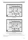
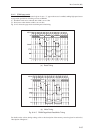
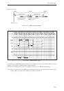
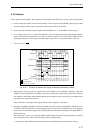
Fig. 8-14-8 DRAM Refresh Timing
For details on the ASR and RP settings, refer to the explanations in section 8.6.2, “Memory Block 1 Control
Register,” and section 8.6.3, “Memory Block 2 Control Register.”
For details on the RERS setting, refer to the explanation in section 8.6.5, “DRAM Control Register.”
Note: When using blocks 1 and 2 as DRAM space simultaneously, the timing (ASR, RP) set in memory control
register 1A/B is used as the refresh timing for both block 1 and block 2.
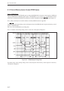
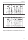
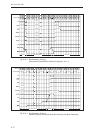
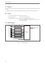
Refresh count value
REFC 0 REFC 0 REFC
REFE bit is set
Refresh is executed
during idle cycle
Refresh is executed with
highest priority
Count interval Count interval
Fig. 8-14-7 DRAM Refresh Operation
MCLK
SYSCLK
An
CAS
RAS2
RAS1
RE
ASR
RERS
“H”
Dn
Refresh
WEn
“H”
“Hi-Z”
ASR RP