


8-bit Timers
10-17
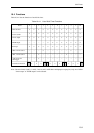
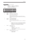
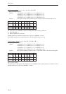
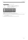
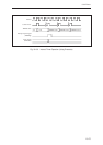
Timer n compare register (n = 4, 5, 6, 7, 8, 9, A, B)
Register symbol: TMnCMP
Address: x'34001034 (n = 4), x'34001035 (n = 5), x'34001036 (n = 6),
x'34001037 (n = 7), x'34001038 (n = 8), x'34001039 (n = 9),
x'3400103A (n = A), x'3400103B (n = B)
Purpose: This is the timer n compare register.
Bit No.76543210
Bit TMn TMn TMn TMn TMn TMn TMn TMn
name CMP7 CMP6 CMP5 CMP4 CMP3 CMP2 CMP1 CMP0
Reset 0 0 0 0 0 0 0 0
Access R/W R/W R/W R/W R/W R/W R/W R/W
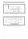
This register sets the PWM output duty ratio.
The duty ratio is (value set in TMnCMP)/(value set in TMnBR + 1).
When data is written to this register, it is written in the compare register buffer.
The set value is loaded from the compare register buffer into the compare register under the following conditions:
(1) When TMnLDE = 1
(2) When an underflow was generated
When this register is read, the value that is actually in the compare register is read.