


Bus Controller (BC)
8-35
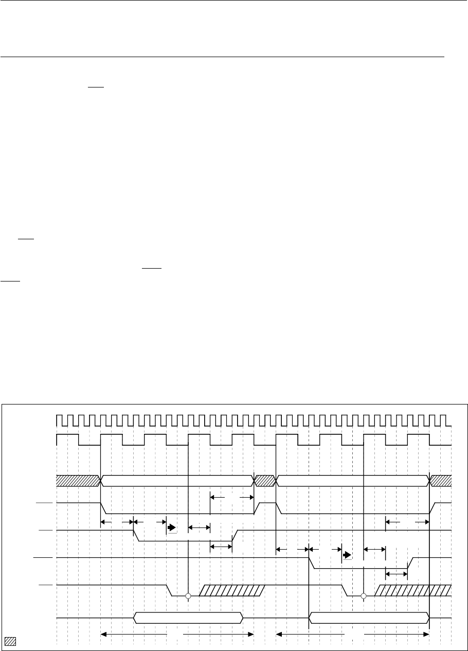
8.13.2 16-bit Bus with Handshaking, in Synchronous Mode and in Address/Data Separate Mode
When using handshaking, bus access starts once synchronization with SYSCLK is achieved, and after the data
acknowledge signal (DK) is asserted, 2 MCLK cycles are consumed by the BC internally and then the access is
completed according to the specified parameters.
The various parameters for external memory access are set in memory control registers 2 and 3, corresponding to
each block.
Handshaking can only be set in synchronous mode.
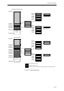
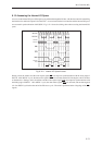
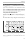
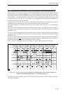
Fig. 8-13-4 is the timing chart in the case of a “16-bit bus with handshaking, in synchronous mode, in address/data
separate mode, and with the frequency of MCLK equal to that of SYSCLK multiplied by four.”
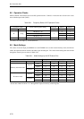
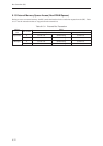
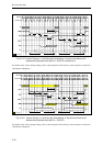
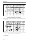
Fig. 8-13-5 is the timing chart in the case of a “16-bit bus with handshaking, in synchronous mode, in address/data
separate mode, and with the frequency of MCLK equal to that of SYSCLK multiplied by two.”
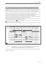
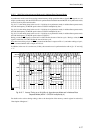
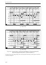
Fig. 8-13-6 is the timing chart in the case of a “16-bit bus with handshaking, in synchronous mode, in address/data
separate mode, and with the frequency of MCLK equal to that of SYSCLK.”
The DK signal connected to the microcontroller should be input so as to be asserted from point EA+DW onward,
and is negated before the next access.
Note that when writing to byte 0, WE0 is asserted and the data is output on D7 to 0, and when writing to byte 1,
WE1 is asserted and the data is output on D15 to 8.
In addition, in the case of a word access (32 bits), the external access is performed twice with A[1] = "0" and A[1]
= "1".
Note: Setting handshaking is prohibited if synchronous mode has not been set.
Note: If handshaking mode is set for memory block 3, the only settings that are permitted are those in which
MCLK is equal to SYSCLK multiplied by 4. Any setting in which MCLK is only twice SYSCLK, or in
which the two frequencies are equal, is prohibited.
Fig. 8-13-4 Access Timing on a 16-bit Bus with Handshaking, in Synchronous Mode and in
Address/Data Separate Mode (MCLK = SYSCLK multiplied by 4)
For details on the various timing settings, refer to the description of the memory control register in section 8.6,
“Description of Registers.”
An
WEn
RE
CSn
MCLK
SYSCLK
Dn
DK
EA
REN
DW
BCE
Read
EA
WEN
DW
BCE
Consumed internally
by the BC
Write
DK detection start
DK detection start
: Undefined
Consumed internally by the BC