


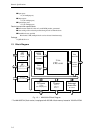

1-7
General Specifications
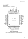
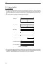
1.4.2 Pin Functions
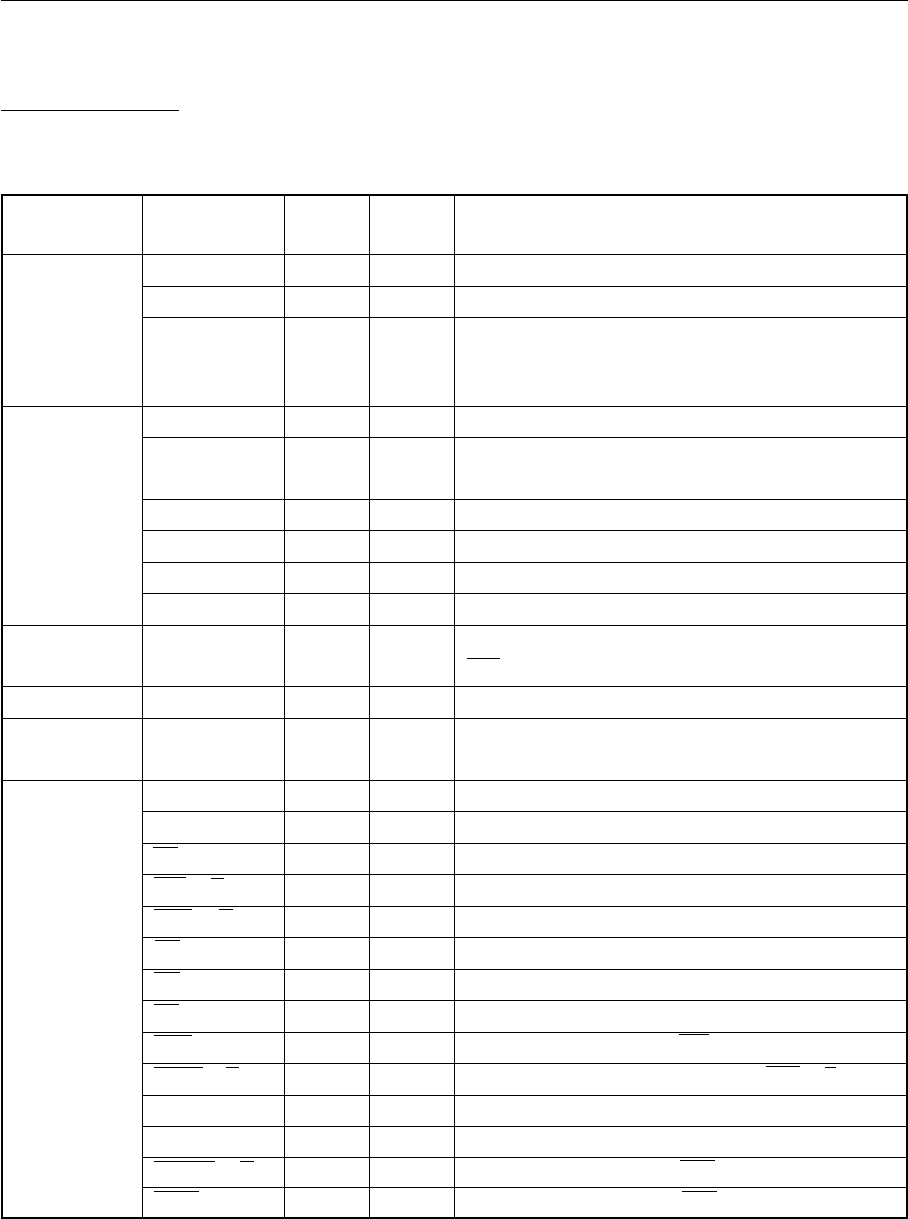
Table 1-4-2 shows the function of each pin of this microcontroller.
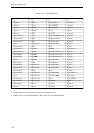
Table 1-4-2 Pin Function Table (1/2)
Category Pin name
Input/ Number
Pin Function
Output of pins
Power supply VDD 8 Digital system power supply (+3.3 V)
VSS 7 Digital system GND
VDD2(VPP) 1 “VDD2” in the case of the MN103001G, “VPP” in the
case of the MN1030F01K. Connect to 5 V or 3.3 V.
Always input 5 V to VPP when writing.
Clock OSCI I 1 Oscillator input
(use input of 3.3 V to 0 V amplitude only.)
OSCO O 1 Oscillator output
(Open when using an external clock input)
SYSCLK O 1 System clock output (multipurpose)
CKSEL I 1 Switch for using/not using PLL
PVDD 1 PLL power supply (+3.3 V)
PVSS 1 PLL GND
Address bus A23 to 0 O 24 Address lines 23 to 0 (multipurpose, A23 also serves as
CS3.)
Data bus D15 to 0 I/O 16 Data lines 15 to 0 (multipurpose)
Address/ ADM15 to 0 I/O (16) Address/Data lines 15 to 0 (A15 to 0 multipurpose)
Data bus
Bus control MMOD1 to 0 I 2 Mode setting signals
signals EXMOD1 to 0 I 2 Extension mode setting (multipurpose)
RE O 1 Memory read signal (multipurpose)
CS3 to 0 O 4 Chip select signals (multipurpose)
WE1 to 0 O 2 Memory write signals (multipurpose)
DK I 1 Data acknowledge signal (multipurpose)
BG O 1 Bus authority release signal (multipurpose)
BR I 1 Bus authority request signal (multipurpose)
CAS O (1) DRAM CAS signals (for 2WE) (multipurpose of A22)
RAS2 to 1 O (2) DRAM RAS signal (multipurpose of CS2 to 1)
AS O (1) Address strobe signal (Also serves as D0.)
RWSEL O (1) Read/write select (Also serves as D1.)
DCAS1 to 0 O (2) DRAM CAS signal (for 2 CAS)
DWE O (1) DRAM write signal (for 2 CAS)