


Bus Controller (BC)
8-58
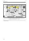
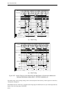
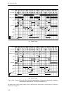
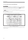
(a) Read Timing
Fig. 8-13-28 Access Timing on a 8-bit Bus with Handshaking in Synchronous Mode and in Address/
Data Multiplex Mode (MCLK = SYSCLK multiplied by 2)
For details on the various timing settings, refer to the description of the memory control register in section 8.6,
“Description of Registers.”
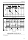
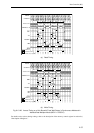
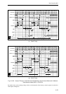
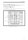
(b) Write Timing
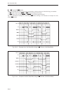
MCLK
SYSCLK
AS
CS2
ASA
ADE
RWSEL
A23* to 16
ADM15 to 0
RE
WE0
ASN
ASA
ADE
ASN
EA
WEN
Write high-order side
Write low-order side
DK
DW
BCE
Consumed internally
by the BC
BCE
EA
WEN
DW
DK detection start
“H”
“0” (“L”)A[0]=0
A[0]=0
A[0]=1
data out
data out A[0]=1
: Undefined
*
“0” (“L”)
Consumed internally
by the BC
DK detection start
: A23 also serves as CS3
: Undefined or Hi-Z
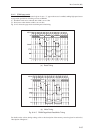
MCLK
SYSCLK
AS
CS2
ASA
ADE
RWSEL
A23* to 16
ADM15 to 0
RE
WE0
ASN
ASA
ADE
ASN
EA
REN
Read high-order side
Read low-order side
DK
DW
DK detection start
BCE
Consumed internally
by the BC
BCE
EA
REN
DW
DK detection start
A[0]=0 A[0]=1
data in
data in
“H”
“0”( )
“L”
A[0]=0 A[0]=1
: Undefined
: A23 also serves as CS3
*
: Undefined or Hi-Z
“0”( )
“L”
Consumed internally
by the BC