


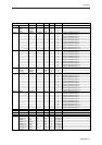
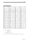
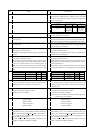
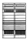


Errors
Page
Corrections
Page
- iv -
P.6-3
P.6-3
P.6-4
P.8-5
P.8-11,
P.8-15
P.8-15,
P.8-20
P.8-35
P.8-35
P.8-36
P.8-41
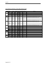
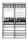
P.6-3
P.6-3
P.6-4
P.8-5
P.8-11,
P.8-15
P.8-15,
P.8-20
P.8-35
P.8-35
P.8-36
P.8-41
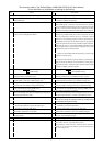
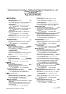
When the reset state is released, SYSCLK, MCLK, and IOCLK are
supplied starting after a certain oscillation stabilization wait time.
Note: For details on the oscillation stabilization wait time, refer to
Chapter 12, “Watchdog Timer.”
Note 1: When a clock is supplied from external, input the clock to the
OSCI pin, and leave the OSCO pin open.
Note 2: The in-circuit emulator (ICE) cannot operate with self-excited
oscillators in the microcontroller. Use the clock generated in the
target system.
When the clock is generated in the target system, supply the
clock to the in-circuit emulator main unit through a buffer with
adequate drive capability. The in-circuit emulator will not operate
correctly if the amplitude of the clock is inadequate, the clock
signal is noisy, or the buffer has inadequate drive capability.
(
Following note is added under the table of "When Using DRAM"
)
Note: When performing ICE trace/emulation in software page
mode, set the CAS parameter to a value of “5” or higher.
(The Setting conditions of EA1 to 0 bit in the table of "When Using
handshaking mode")
00: prohibited
01: 1MCLK
10: 2MCLK
11: 3MCLK
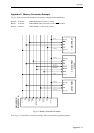
(Following sentence is added to 13th line.)
_____
The DK signal connected to the microcontroller should be input so
as to be asserted from point EA+DW onward, and is negated before
the next access.
____
(In figure 8-13-4, the DK signal asserted by the read access was
changed so as to be negated before the write access. )
____
(In figure 8-13-5 and 8-13-6, the DK signal asserted by the read
access was changed so as to be negated before the write access.
____ ____
Moreover, the signal name, CSn was changed to CS2. )
(Following sentence is added to 20th line.)
_____
The DK signal connected to the microcontroller should be input so
as to be asserted from point EA+DW onward, and is negated before
the next access.
When the reset state is released, SYSCLK, MCLK, and IOCLK are
supplied starting after a certain oscillation stabilization wait time.
Note: • When a clock is supplied from external, input the clock to
the OSCI pin, and leave the OSCO pin open.
• For details on the oscillation stabilization wait time, refer to
Chapter 12, “Watchdog Timer.”
(The Setting condition of EA1 to 0 bit in the table of "When Using
handshaking mode")
00: 0MCLK
~
~
11: 3MCLK
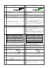
8 fosci 15 MHz
Input frequency range PLL
When using
When not using
8 fosci 30 MHz
8 MHz fosci 18 MHz
Input frequency range PLL
When using
8 MHz fosci 20 MHz
When not using
8
fosci
15 8
fsys
15
Multiple
fosci(MHz)
fsys(MHz) fc (MHz) fio (MHz)
Multiple
Frequency Frequency Frequency
Multiple
32
fc
60
*
8
fio
15
8
fosci
30 4
fsys
15 4
fc
15 1
fio
3.751/21/2 1/8
8
fc
15 2
fio
3.751
1
1/4
16
fc
30 4
fio
7.52 1/2
41
8
fsys
18
Multiple
fosci(MHz)
fsys(MHz) fc (MHz) fio (MHz)
Multiple
Frequency Frequency Frequency
Multiple
32
fc
60
*
8
fio
15
4
fsys
10 4
fc
10 1
fio
2.51/21/2 1/8
8
fc
18 2
fio
4.51
1
1/4
16
fc
36 4
fio
92 1/2
41
8
fsys
15
1
8
fosci
20
8
fosci
18
8
fosci
15
Function
Oscillator input pin (when using PLL: 8
MHz to
15
M
Hz; when
not using PLL: 8
MHz to
30
M
Hz)
Oscillator output pin (when using PLL: 8
MHz to
15
M
Hz; when
not using PLL: 8
MHz to
30
M
Hz)
Function
Oscillator input pin (when using PLL: 8
MHz to
18
M
Hz; when
not using PLL: 8
MHz to
20
M
Hz)
Oscillator output pin (when using PLL: 8
MHz to
18
M
Hz; when
not using PLL: 8
MHz to
20
M
Hz)