


Bus Controller (BC)
8-22
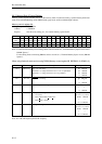
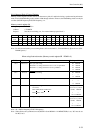
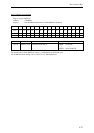
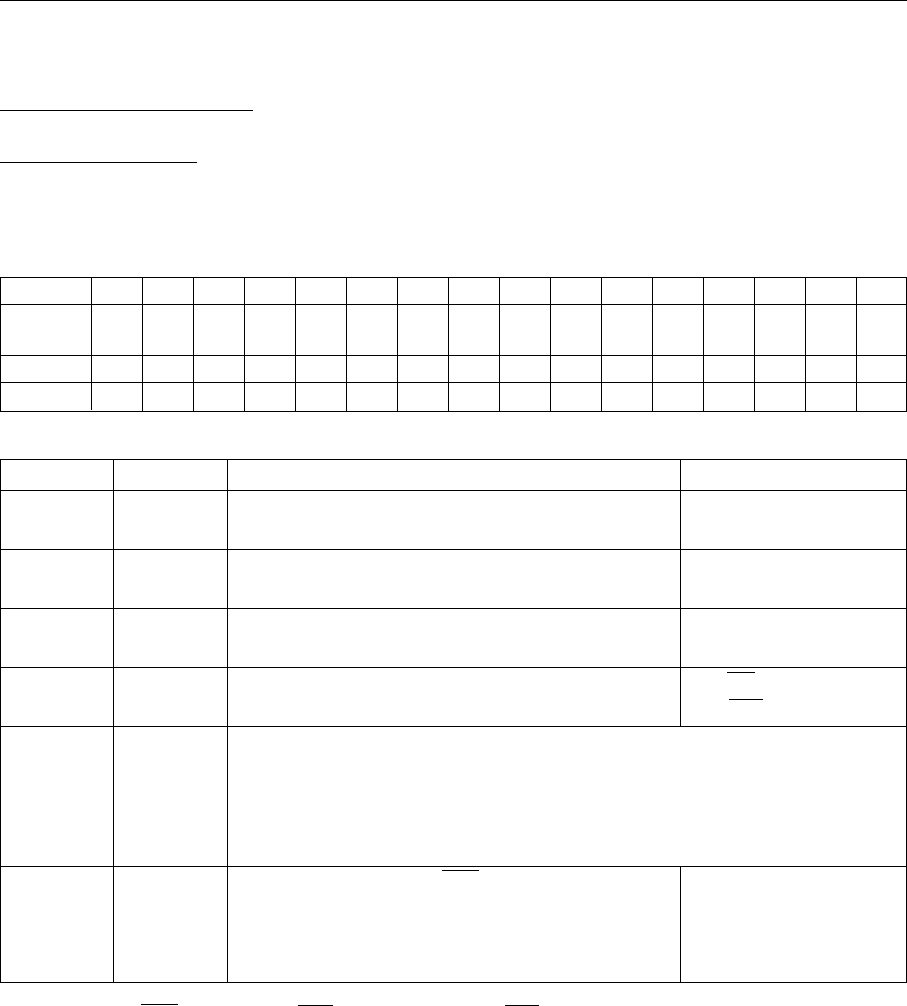
8.6.5 DRAM control register
DRAM control register
Register symbol: DRAMCTR
Address: x'32000040
Purpose: Stores various DRAM mode settings when DRAM is connected.
Bit No. 15 14 13 12 11 10 9876543210
Bit
––––
RERS RERS RERS RERS SIZE SIZE
––BWC
REFE PAGE
DRAM
name 321010 E
Reset 0000001100000000
Access RRRRR/WR/WR/WR/WR/WR/WRRR/WR/WR/WR/W
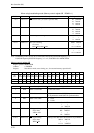
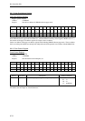
Bit No. Bit name Description Setting conditions
0 DRAME DRAM control circuit enable 0: Disabled
1: Enabled
1 PAGE Page mode enable 0: Disabled
1: Enabled
2 REFE Refresh enable 0: Disabled
1: Enabled
3 BWC Byte wide control 0: 2 WE control
1: 2 CAS control
7 to 6 SIZE1 to 0 DRAM size
00: Shift the address 9-bits to the low-order side and use as the row address
01: Shift the address 10-bits to the low-order side and use as the row address
10: Shift the address 11-bits to the low-order side and use as the row address
11: Shift the address 8-bits to the low-order side and use as the row address
11 to 8 RERS3 to 0 Number of MCLK while RAS is asserted 0000: prohibited
in the refresh cycle. 0001: 1MCLK
1111: 15MCLK
For details on the RAS hold time, the RAS precharge cycle, the CAS pulse width, the row address setup timing, the
column address output timing, and the column address setup timing, refer to memory control registers 1A/B and
2A/B.
For the timing charts when using DRAM, refer to section 8.14, “External Memory Space Access (DRAM Spaces).”
~
~