


Internal Flash Memory
16-8
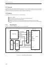
16.6 On-board Write Mode
In on-board write mode, flash memory is overwritten by manipulating the control registers through software.
Table 16-6-1 lists the control registers to be used in on-board write mode.
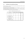
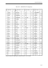
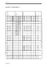
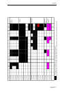
Table 16-6-1 Flash Memory Register List
*1: FLMODR[3:0] uses the values of MMOD1 and 0 and EXMOD1 and 0, and FLMODR[7:4] is x'0.
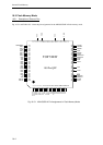
If an on-board write is performed, some bus control signal pins (except for RE, WE1, and WE0) and the address
and data signal pins operate.
The pins that operate are listed below:
The RE, WE1, and WE0 signal pins each output a high signal.
If the pins are set for other signals by the I/O port register settings, they operate in accordance with the register
settings.
Design the board of any external device that is to be connected to above signal pins in such a way that no difficulty
will be encountered even if the above signal pins do operate.
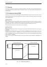
AS
RWSEL
ADM [15:0]
Address/data separate
A [12:0]
D [15:0]
Address/data multiplex
Address Registername Symbol
Number of bits
Initial value Access size
x'34010000
Flash on-board rewrite control register FCREG 16 x'0017 8, 16
x'34010004
Flash data register FDREG 16 x'0000 8, 16
x'34010008
Flash address register (Lower) FAREG 16 x'0000 8, 16
x'3401000C
Flash address register (Upper) FAREGEX 16 x'0000 8, 16
x'34010010
Flash on-board rewrite enable register FBEWER 16 x'0000 8, 16
x'34010014 Flash memory mode register
FLMODR 8 *1 8