


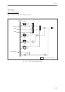
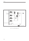
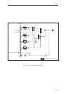
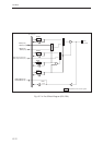
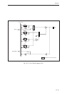
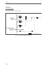
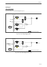

I/O Ports
15-37
15.7.3 Pin Configurations
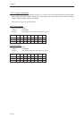
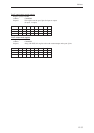
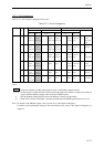
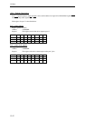
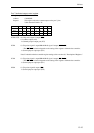
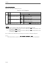
Table 15-7-1 shows the pin configurations for port 5.
Table 15-7-1 Port 5 Configuration
Port Pin P5n P5nM = "1" P5nM = "0"
No. P5nS = "1" P5nS = "0" P5nS = "1" P5nS = "0"
P5nD = "1"
P5nD = "0"
P5nD ="1" P5nD ="0" P5nD = "1"
P5nD = "0"
Port 5 67 P50 General- General- P50 General- General- TM0IO Timer 0 Timer 0 SBT2 Serial 2
purpose purpose purpose purpose or timer or timer 8 *
5
transfer
output port input port output port input port 8 output input clock input/
*
1
output
66 P51 General- General- P51 General- General- TM1IO Timer 1 Timer 1 SBI2 Serial 2
purpose purpose purpose purpose or timer or timer 9 data input
output port input port output port input port 9 output input
*
2
65 P52 General- General- P52 General- General- TM2IO Timer 2 Timer 2 SBO2 Serial 2
purpose purpose purpose purpose or timer or timer A *
5
data
output port input port output port input port A output input input/output
*
3
64 P53 General- General- TM11IO Timer 11 Timer 11 TM3IO Timer 3 Timer 3 SBT3 Serial 3
purpose purpose output input or timer or timer B *
6
transfer
output port input port B output input clock input
*
4
63 P54 General- General- TM12IO Timer 12 Timer 12 TM4IO Timer 4 Timer 4 SBI3 Serial 3
purpose purpose output input output input data input
output port input port
62 P55 General- General- TM13IO Timer 13 Timer 13 TM5IO Timer 5 Timer 5 SBO3 Serial 3
purpose purpose output input output input data output
output port input port
[Note]
: When reset (whether in address/data separate mode or address/data multiplex mode)
*1 to *4 : Set the respective output selections for timer 3/timer B output, timer 2/timer A output, timer 1/timer 9
output, and timer 0/timer 8 output in the 8-bit timer TMOSL register.
*5 : The input/output settings depend on the serial interface 2 settings and the timing.
*6 : When serial 3 transfer clock input is selected, the P53D bit in the P5DIR register must be set to "0".
Note: For details on the TMOSL register, refer to section 10.5, "Description of Registers."
For details on the input/output settings for the serial interface pins, refer to "Description of Registers" in
chapter 13.