


Bus Controller (BC)
8-62
8.14 External Memory Space Access (DRAM Space)
8.14.1 DRAM Space
Blocks 1 and 2 can be used as DRAM space by setting the BnDRAM bits in memory control registers 1B/2B and
setting the DRAME bit in DRAM control register. The DRAM bus cycle is always not synchronized the external
clock (but is synchronized with MCLK), and performs address multiplexed output, RAS/CAS signal output, etc.
Note: When common pins are used for addresses and data, DRAM cannot be supported.
The RAS/CAS signal output timing can be set through software in the DRAM control register and memory control
registers 1A/B and 2A/B.
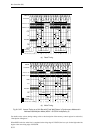
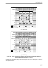
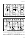
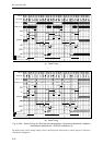
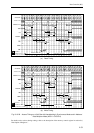
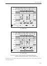
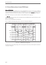
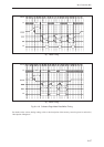
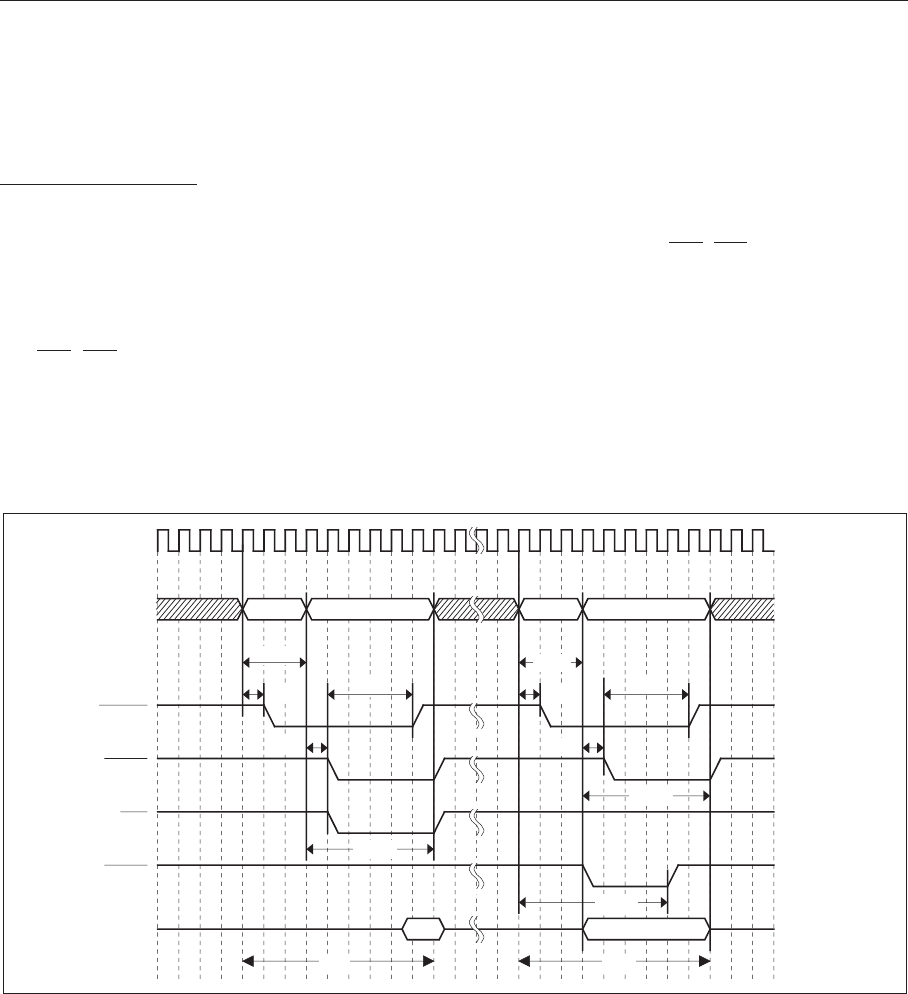
Fig. 8-14-1 shows the DRAM access timing chart.
Note: For details on the timing settings, refer to section 8.6, “Description of Registers.”
MCLK
ASR
CAO
An
RASn
CAS
RE
Dn
CAS
ASC
Column
RSH
WEn
ASC
Column
CAO
ASR
CAS
WEN
Row Row
RSH
Read
Write
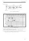
Fig. 8-14-1 DRAM Access Timing Chart
For details on the various timing settings, refer to the description of the memory control register in section 8.6,
“Description of Registers.”