


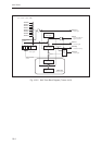
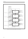

8-bit Timers
10-12
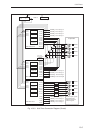
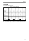
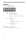
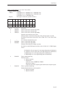
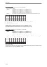
Timer n mode register (n = 0, 1, 2, 3)
Register symbol: TMnMD
Address: x'34001000 (n=0), x'34001001 (n=1),
x'34001002 (n=2), x'34001003 (n=3)
Purpose: This register controls the operation of timer n.
Bit No.76543210
Bit TMn TMn
---
TMn TMn TMn
name CNE LDE CK2 CK1 CK0
Reset 0 0 0 0 0 0 0 0
Access R/W R/W R R R R/W R/W R/W
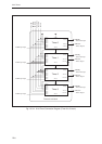
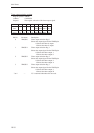
Bit No. Bit name Description
0 TMnCK0 Timer n clock source selection flag (LSB)
1 TMnCK1 Timer n clock source selection flag
2 TMnCK2 Timer n clock source selection flag (MSB)
These bits select the timer clock source.
When pin input is selected, the rising edge of the pin input signal is counted.
For details on each timer clock sources, refer to Table 10-5-3, "8-bit Timer Clock
Sources."
5 to 3 – "0" is returned when these bits are read.
6 TMnLDE Timer n initialization flag
Initializes timer n.
0: Normal operation
1: Initialize
Loads the value in TMnBR into TMnBC. Resets timer output n to "L"
level.
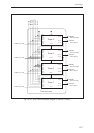
7 TMnCNE Timer n output enable flag
Enables/disables the timer n count operation.
0: Operation disabled
1: Operation enabled
[Note]
When setting TMnCNE to "1", do so while TMnLDE is set to "0".
When setting TMnLDE to "1", do so while TMnCNE is set to "0".
Operation is not guaranteed if TMnCNE and TMnLDE are both set to "1" at the same time.