


Serial Interface
13-22
If the above procedures do not satisfy the AC timing of the device that is connected, send the stop sequence
according to the procedure described below.
(1)' SBT pin setting
Set the SBT pin as a general-purpose input port.
When the pin switches to a general-purpose input port, SCL goes high.
(2)' SBO pin setting
Set the SBO pin as a general-purpose input port.
When the pin switches to a general-purpose input port, SDA goes high and the stop sequence is generated.
(3)' Transmission/reception disable
Disable the transmission operation and the reception operation.
(Set SC0TXE and SC0RXE to "0". Be sure to always perform this step every time after the stop sequence is
sent.)
(4)' I/O port setting
To perform further transmission/reception operations, set the I/O ports to SBT and SBO.
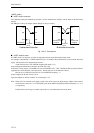
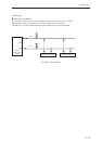
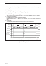
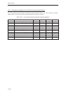
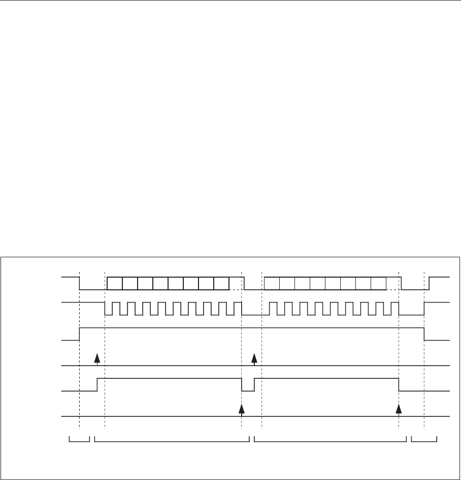
Fig. 13-2-15 Timing Chart (11)
bp7 bp6 bp5 bp4 bp3 bp2 bp1 bp0 Ack bp7 bp6 bp5 bp4 bp3 bp2 bp1 bp0 Ack
(A)
(B)
(C)
Start sequence send Data transmission/reception
(B)
Stop sequence send
SBO pin
(SDA)
SBT pin
(SCL)
SC0IIC flag
Data write
SC0TXF flag
Interrupt request
(set to “transmission
end”)
Data transmission/reception