Memory Modes
4-3
4.2 Memory Mode Pin Processing
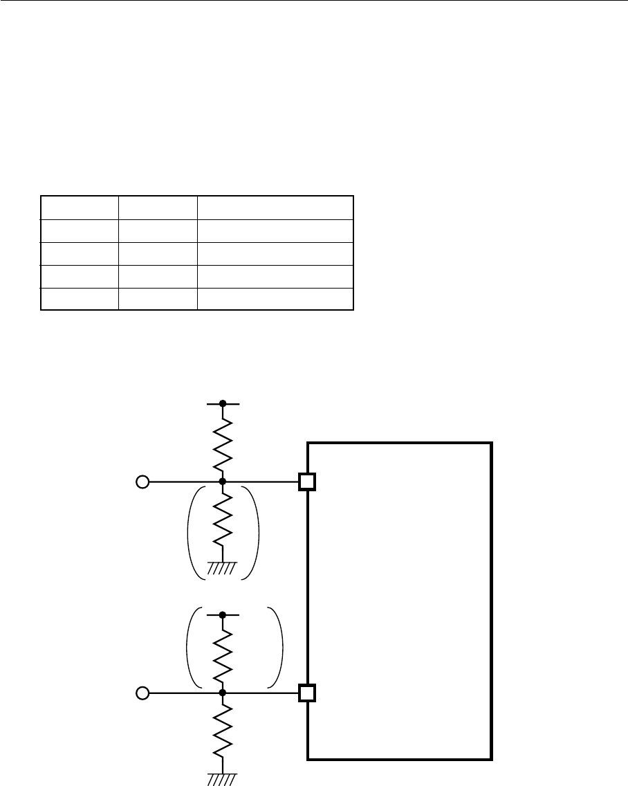
Fix the input levels for the memory mode pins (MMOD0,1) as shown in Table 4-2-1 and Fig. 4-2-1 with pull-up/
pull-down resistors.
For details on the pull-up/pull-down resistance, refer to “High-speed Serial Control Card Operation Manual”.
Table 4-2-1 Memory Mode Setting
MMOD1 MMOD0 Memory mode
L H Extension memory mode
H L Processor mode
L L Setting prohibited
H H Setting prohibited
For details on the memory mode settings for onboard writing of flash memory in the MN1030F01K, refer to
chapter 16, “Internal Flash Memory”.
Fig. 4-2-1 Memory Mode Pin Connection Diagram
Note that the memory mode pins (MMOD0,1) also serve as serial interface pins for debugging and for onboard
writing of flash memory in the MN1030F01K. The memory mode pins (MMOD0 and 1) are normally input pins,
but when they are connected to the serial interface for debugging and for onboard writing of flash memory in the
MN1030F01K, they become N ch (when pulled up) or P ch (when pulled down) open drain input/output pins.
♦ Direct inquires for details on the serial interface for debugging and for onboard writing of flash memory in the
MN1030F01K to the contact indicated at the end of this manual.
MMOD0
(SDATA)
MMOD1
(SCLOCK)
Pull up or pull down
R'
R
R'
R
VDD
VDD
MN103001G
/MN1030F01K


