


16-bit Timers
11-6
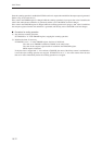
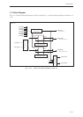
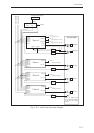
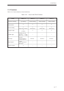
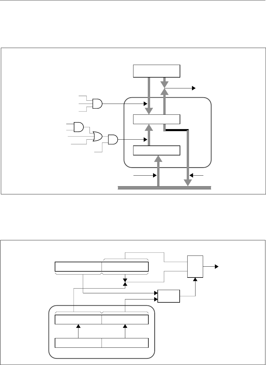
Fig. 11-3-4 shows the block diagram for the timer 10 compare/capture registers.
Fig. 11-3-4 Timer 10 Compare/Capture Register Block Diagram
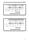
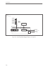
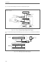
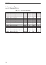
Fig. 11-3-5 shows the block diagram for the PWM output section when timer 10 is set to PWM mode with additional
bits.
Fig. 11-3-5 PWM Output Section Block Diagram
TM10BC
TM10CA
(TM10CB)
Additional bit
control
Underflow
R
S
Low-order 8 bits
High-order 8 bits Low-order 8 bits
High-order 8 bits
TMnOUT
PWM output
High-order 8 bits Low-order 8 bits
Compare/capture
register
Compare register buffer
Timer 10 compare/capture registers
( TM10CA, TM10CB )
Compare/capture register
Compare register buffer
Data bus
Register write
Register read
Double-buffer mode
Load timing
Single-buffer mode
Initialization flag (TM10LDE)
Compare register mode
Capture register mode
Capture enable
Capture timing
Compare/capture A (B)
register
TM10CA (TM10CB)
Match interrupt
request
TM10BC
Binary counter