


159
CHAPTER 7 CLOCK GENERATOR
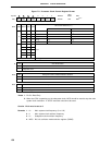
The fastest instruction of the
µ
PD78075F and 78075FY Subseries can be executed in two clocks of the CPU clock.
The relationship between the CPU clock (fCPU) and the minimum instruction execution time is shown in Table 7-2.
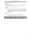
Table 7-2. Relationship Between CPU Clock and Minimum Instruction Execution Time
CPU Clock (fCPU) Minimum Instruction Execution Time: 2/fCPU
fX 0.4
µ
s
fX/2 0.8
µ
s
fX/2
2
1.6
µ
s
fX/2
3
3.2
µ
s
fX/2
4
6.4
µ
s
fX/2
5
12.8
µ
s
fXT/2 122
µ
s
fX = 5.0 MHz, fXT = 32.768 kHz
f
X : Main system clock oscillation frequency
fXT: Subsystem clock oscillation frequency
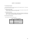
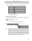
(2) Oscillation mode selection register (OSMS)
This register specifies whether the clock output from the main system clock oscillator without passing through
the scaler is used as the main system clock, or the clock output via the scaler is used as the main system
clock.
OSMS is set with 8-bit memory manipulation instruction.
RESET input sets OSMS to 00H.
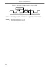
Figure 7-4. Oscillation Mode Selection Register Format
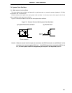
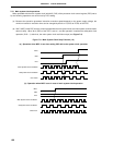
Caution 1. Writing to OSMS should be performed only immediately after reset signal release and before
peripheral hardware operation starts. As shown in Figure 7-5 below, writing data (including
same data as previous) to OSMS cause delay of main system clock cycle up to 2/f
x during
the write operation. Therefore, if this register is written during the operation, in peripheral
hardware which operates with the main system clock, a temporary error occurs in the count
clock cycle of timer, etc. Also, when switching the oscillation mode, the clock supplied to
the CPU is switched as well as the clock supplied to the peripheral hardware. Therefore, it
is recommended that the instruction for writing to OSMS be executed only once after
releasing the reset and before operating the peripheral hardware.
MCS
Main System Clock Scaler Control
0
1
Scaler used
Scaler not used
000 0OSMS FFF2H
765432Symbol
1
0 MCS
0
0
Address
After
Reset
R/W
00H W
0