


294
CHAPTER 16 SERIAL INTERFACE CHANNEL 0 (
µ
PD78058F SUBSERIES)
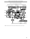
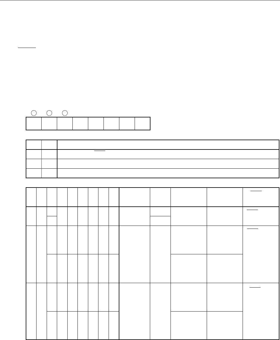
(2) Serial operating mode register 0 (CSIM0)
This register sets serial interface channel 0 serial clock, operating mode, operation enable/stop wake-up
function and displays the address comparator match signal.
CSIM0 is set with a 1-bit or 8-bit memory manipulation instruction.
RESET input sets CSIM0 to 00H.
Caution Do not switch the operating mode (3-wire serial I/O/ 2-wire serial I/O/SBI) while operation of
serial interface channel 0 is enabled. If switching the operation mode, first terminate the
serial operation, then carry out switching.
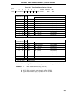
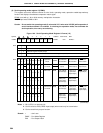
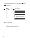
Figure 16-4. Serial Operating Mode Register 0 Format (1/2)
(Continued)
Notes 1. Bit 6 (COI) is a read-only bit.
2. Can be used as P25 (CMOS input/output) when used only for transmission.
3. Can be used freely as port function.
Remark × : don’t care
PMXX : Port Mode Register
PXX : Port Output Latch
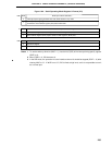
SBI mode
65432107
Symbol
CSIM0 CSIE0 COI WUP
CSIM04 CSIM03 CSIM02 CSIM01 CSIM00
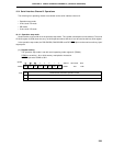
CSIM01
0
1
Serial Interface Channel 0 Clock Selection
Input Clock to SCK0 pin from off-chip
8-bit timer register 2 (TM2) output
0
0
SCK0 (CMOS
input/output)
R/W
1 Clock specified with bits 0 to 3 of timer clock select register 3 (TCL3)
CSIM
04
0
1
CSIM00
×
0
1
FF60H 00H R/W
Note 1
Address After Reset R/W
R/W
CSIM
03
CSIM
02
PM25 P25 PM26 P26
PM27
P27
Operation
Mode
Start Bit
SIO/SB0/P25
Pin Function
SO0/SB1/P26
Pin Function
SCK0/P27
Pin Function
×
10
×
0
×
0
0
×
0
×
0
0
1
1
Note 3 Note 3
Note 3 Note 3
MSB
P25 (CMOS
input/output)
SB0 (N-ch
open-drain
input/output)
SB1 (N-ch
open-drain
input/output)
P26 (CMOS
input/output)
1
MSB
LSB
1 × 0001
Note 2
3-wired serial
l/O mode
SI0
(Input)
SO0
(CMOS output)
SCK0 (CMOS
input/output)
Note 2
2-wired serial
l/O mode
0
SCK0 (N-ch
open-drain
input/output)
1
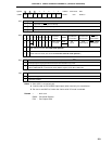
11
×
0
×
0
0
×
0
×
0
0
1
1
Note 3 Note 3
Note 3 Note 3
MSB
P25 (CMOS
input/output)
SB0 (N-ch
open-drain
input/output)
SB1 (N-ch
open-drain
input/output)
P26 (CMOS
input/output)
Note 2