


383
CHAPTER 17 SERIAL INTERFACE CHANNEL 0 (
µ
PD78058FY SUBSERIES)
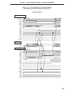
(4) Reception completion of salve
In the reception completion processing of the slave, check the bit 3 (CMDD) of the serial bus interface
control register (SBIC) and bit 6 (COI) of the serial operation mode register 0 (CSIM0) (when CMDD = 1).
This is to avoid the situation where the slave cannot judge which of the start condition and data comes first
and therefore, the wake-up condition cannot be used when the slave receives the undefined number of
data from the master.
17.4.6 Restrictions in I
2
C bus mode
The following restrictions are applied to the
µ
PD78058FY Subseries.
• Restrictions when used as slave device in I
2
C bus mode
Subject:
µ
PD78056FY, 78058FY, 78P058FY, IE-78064-R-EM
Note
, IE-780308-R-EM,
IE-780308-NS-EM1
Note Maintenance product
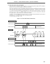
Description: If the wake-up function is executed (by setting the bit 5 of the serial operating mode
register 0 (CSIM0) to 1) in the serial transfer status
Note
, the
µ
PD78058FY subseries
checks the address of the data between the other slave and master. If that data hap-
pens to coincide with the slave address of the
µ
PD78058FY subseries, the
µ
PD78058FY
subseries takes part in communication, destroying the communication data.
Note The serial transfer status is the status since data has been written to the serial I/
O shift register 0 (SIO0) until the interrupt request flag (CSIIF0) is set to 1 by
completion of the serial transfer.
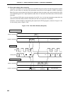
Preventive measure: The above phenomenon can be avoided by modifying the program.
Before executing the wake-up function, execute the following program that clears the
serial transfer status. When executing the wake-up function, do not execute an instruc-
tion that writes data to SIO0. Even if such an instruction is not executed, data can be
received while the wake-up function is executed.
This program releases the serial transfer status. To release the serial transfer status,
the serial interface channel 0 must be once disabled (by clearing the CSIE0 flag (bit 7 of
the serial operating mode register (CSIM0) to 0). If the serial interface channel 0 is
disabled in the I
2
C bus mode, however, the SCL pin outputs a high level, and SDA0
(SDA1) pin outputs a low level, affecting communication of the I
2
C bus. Therefore, this
program makes the SCL and SDA0 (SDA1) pins go into a high-impedance state to pre-
vent the I
2
C bus from being affected.
In this example, the SDA0 (/P25) pin is used as a serial data input/output pin. When the
SDA1 (/P26) is used, take P2.5 and PM2.5 in the program example below as P2.6 and
PM2.6.
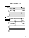
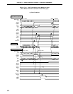
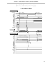
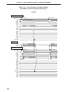
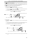
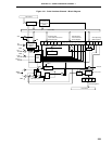
For the timing of each signal when this program is executed, refer to Figure 17-22.