


343
CHAPTER 17 SERIAL INTERFACE CHANNEL 0 (
µ
PD78058FY SUBSERIES)
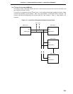
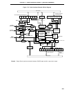
(3) SO0 latch
This latch holds SI0/SB0/SDA0/P25 and SO0/SB1/SDA1/P26 pin levels. It can be directly controlled by
software.
(4) Serial clock counter
This counter counts the serial clocks to be output and input during transmission/reception and to check whether
8-bit data has been transmitted/received.
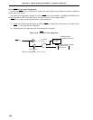
(5) Serial clock control circuit
This circuit controls serial clock supply to the serial I/O shift register 0 (SIO0). When the internal system clock
is used, the circuit also controls clock output to the SCK0/SCL/P27 pin.
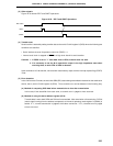
(6) Interrupt signal generator
This circuit controls interrupt request signal generation. It generates interrupt request signals according to
the settings of interrupt timing specification register (SINT) bits 0 and 1 (WAT0, WAT1) and serial operation
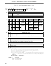
mode register 0 (CSIM0) bit 5 (WUP), as shown in Table 17-3.
(7) Acknowledge output circuit and stop condition/start condition/acknowledge detector
These two circuits output and detect various control signals in the I
2
C mode.
These do not operate in the 3-wire serial I/O mode and 2-wire serial I/O mode.