


290
CHAPTER 16 SERIAL INTERFACE CHANNEL 0 (
µ
PD78058F SUBSERIES)
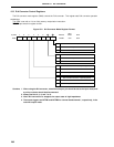
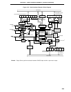
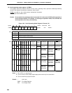
(1) Serial I/O shift register 0 (SIO0)
This is an 8-bit register to carry out parallel/serial conversion and to carry out serial transmission/reception
(shift operation) in synchronization with the serial clock.
SIO0 is set with an 8-bit memory manipulation instruction.
When bit 7 (CSIE0) of serial operating mode register 0 (CSIM0) is 1, writing data to SIO0 starts serial operation.
In transmission, data written to SIO0 is output to the serial output (SO0) or serial data bus (SB0/SB1). In
reception, data is read from the serial input (SI0) or SB0/SB1 to SIO0.
Note that, if a bus is driven in the SBI mode or 2-wire serial I/O mode, the bus pin must serve for both input
and output. Thus, in the case of a device for reception, write FFH to SIO0 in advance (except when address
reception is carried out by setting bit 5 (WUP) of CSIM0 to 1).
In the SBI mode, the busy state can be cleared by writing data to SIO0. In this case, bit 7 (BSYE) of the serial
bus interface control register (SBIC) is not cleared to 0.
RESET input makes SIO0 undefined.
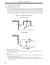
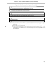
(2) Slave address register (SVA)
This is an 8-bit register to set the slave address value for connection of a slave device to the serial bus.
This register is not used in the 3-wire serial I/O mode.
SVA is set with an 8-bit memory manipulation instruction.
The master device outputs a slave address for selection of a particular slave device to the connected slave
device. These two data (the slave address output from the master device and the SVA value) are compared
with an address comparator. If they match, the slave device has been selected. In that case, bit 6 (COI) of
serial operating mode register 0 (CSIM0) becomes 1.
Also, by setting bit 4 (SVAM) of the interrupt timing instruction register (SINT) at (1), the address can be
compared with the higher order 7 bits, with the LSB being masked.
If no match is detected when the address is received, bit 2 (RELD) of the serial bus interface control register
(SBIC) is cleared to 0. Furthermore, when in the SBI mode, the wake up function can be used by setting bit
5 (WUP) of CSIM0 at (1). In this case, the interrupt request signal (INTCSI0) is generated only when the slave
address output by the master coincides with the value of SVA, and it can be learned by this interrupt request
that the master requests for communication. If the bit 5 (SIC) of the interrupt timing specify register (SINT)
is set to 1, the wake-up function cannot be used even if WUP is set to 1 (an interrupt request signal is generated
when bus release is detected). To use the wake-up function, clear SIC to 0.
Further, errors can be detected using the SVA when sending data as a master or slave while in the SBI mode
or the 2-wire serial I/O mode.
RESET input makes SVA undefined.