


372
CHAPTER 17 SERIAL INTERFACE CHANNEL 0 (
µ
PD78058FY SUBSERIES)
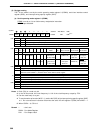
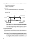
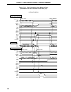
(5) Pin configurations
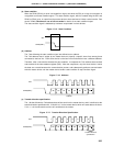
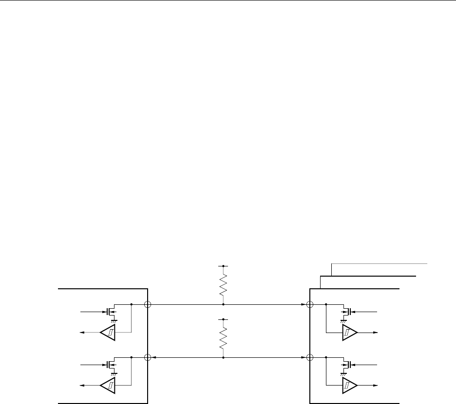
The configurations of the serial clock pin SCL and the serial data bus pins SDA0 (SDA1) are shown below.
(a) SCL
Pin for serial clock input/output dual-function pin.
<1> Master ..... N-ch open-drain output
<2> Slave ....... Schmitt input
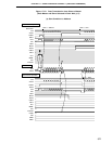
(b) SDA0 (SDA1)
Serial data input/output dual-function pin.
Uses N-ch open-drain output and Schmitt-input buffers for both master and slave devices.
Note that pull-up resistors are required to connect to both serial clock line and serial data bus line,
because open-drain buffers are used for the serial clock pin (SCL) and the serial data bus pin (SDA0 or
SDA1) on the I
2
C bus.
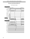
Figure 17-21. Pin Configuration
Caution It is necessary for the N-ch open-drain output to be set in the high impedance state when
receiving data, so set 1 in bit 7 (BSYE) of the serial bus interface control register (SBIC)
in advance and write FFH in serial I/O shift register 0 (SIO0).
However, when the wake up function is used (when bit 5 (WUP) of serial operation mode
register 0 (CSIM0) is set), do not write FFH in SIO0 before reception. Even if FFH is not
written in SIO0, the N-ch open-drain output is always in the high impedance state.
(6) Address match detection method
In the I
2
C mode, the master can select a specific slave device by sending slave address data.
CSIIF0 is set if the slave address transmitted by the master coincides with the value set to the slave
address register (SVA) when a slave device address has a slave register (SVA), and the wake-up function
specify bit (WUP) = 1 (CSIIF0 is also set when the stop condition is detected).
When using the wake-up function, set SIC to 1.
Caution Be sure to set the WUP bit to 1 before the master device sends slave address data to slave
devices. Each slave device recognizes whether the slave device is selected or not by
master device by comparing the content of the SVA register (which is in each slave device)
and the slave address data, which is sent by master device immediately after the start
condition signal. Only if the WUP bit has been set to 1 when they match, the slave device
generates INTCSI0 signal.
AV
DD
AV
DD
SCL
SDA0(SDA1)
Master Device
Clock Output
(Clock Input)
Data Output
Data Input
Slave Devices
(Clock Output)
Clock Input
Data Output
Data Input
SCL
SDA0(SDA1)
AV
SS
AV
SS
AV
SS
AV
SS