


361
CHAPTER 17 SERIAL INTERFACE CHANNEL 0 (
µ
PD78058FY SUBSERIES)
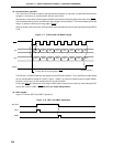
12345678
SCK0
D7 D6 D5 D4 D3 D2 D1 D0
SB0 (SB1)
CSIIF0
Transfer Start at the Fallin
g
Ed
g
e of SCK0
End of Transfer
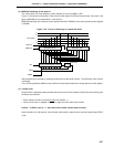
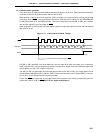
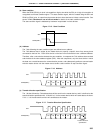
(2) Communication operation
The 2-wire serial I/O mode is used for data transmission/reception in 8-bit units. Data transmission/reception
is carried out bit-wise in synchronization with the serial clock.
Shift operation of the serial I/O shift register 0 (SIO0) is carried out in synchronization with the falling edge
of the serial clock (SCK0). The transmit data is held in the SO0 latch and is output from the SB0/SDA0/P25
(or SB1/SDA1/P26) pin on an MSB-first basis. The receive data input from the SB0 (or SB1) pin is latched
into the shift register at the rising edge of SCK0.
Upon termination of 8-bit transfer, the shift register operation stops automatically and the interrupt request
flag (CSIIF0) is set.
Figure 17-11. 2-Wire Serial I/O Mode Timings
Pin SB0 (or SB1) specified in the serial data bus is an N-ch open-drain input and output, so it is necessary
to pull it up externally. It is also necessary to set the N-ch open-drain output in the high impedance state when
receiving data, so write FFH in SIO0 in advance.
The SB0 (or SB1) pin generates the SO0 latch status and thus the SB0 (or SB1) pin output status can be
manipulated by setting bit 0 (RELT) and bit 1 (CMDT) of serial bus interface control register (SBIC). However,
do not carry out this manipulation during serial transfer.
Control the SCK0 pin output level in the output mode (internal system clock mode) by manipulating the P27
output latch (refer to 17.4.7 SCK0/SCL/P27 pin output manipulation).