


254
CHAPTER 12 CLOCK OUTPUT CONTROL CIRCUIT
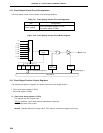
12.2 Clock Output Control Circuit Configuration
The clock output control circuit consists of the following hardware.
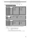
Table 12-1. Clock Output Control Circuit Configuration
Item Configuration
Timer clock select register 0 (TCL0)
Port mode register 3 (PM3)
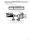
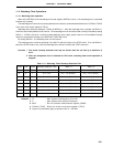
Figure 12-2. Clock Output Control Circuit Block Diagram
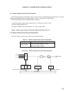
12.3 Clock Output Function Control Registers
The following two types of registers are used to control the clock output function.
• Timer clock select register 0 (TCL0)
• Port mode register 3 (PM3)
(1) Timer clock select register 0 (TCL0)
This register sets PCL output clock.
TCL0 is set with a 1-bit or 8-bit memory manipulation instruction.
RESET input sets TCL0 to 00H.
Remark Besides setting PCL output clock, TCL0 sets the 16-bit timer register count clock.
Control register
Internal Bus
f
XX
f
XX
/2
f
XX
/2
2
f
XX
/2
3
f
XX
/2
4
f
XX
/2
5
f
XX
/2
6
f
XX
/2
7
f
XT
CLOE TCL03 TCL02 TCL01 TCL00
P35
Output Latch
Synchronizing
Circuit
4
PM35
Selector
Timer Clock Select Register 0
Port Mode Register 3
PCL/P35