


39
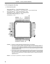
CHAPTER 1 OUTLINE (
µ
PD78058F SUBSERIES)
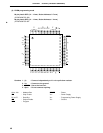
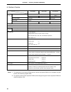
Pin Identifications
A8 to A15 : Address Bus
AD0 to AD7 : Address/Data Bus
ANI0 to ANI7 : Analog Input
ANO0, ANO1 : Analog Output
ASCK : Asynchronous Serial Clock
ASTB : Address Strobe
AV
DD : Analog Power Supply
AVREF0, 1 : Analog Reference Voltage
AVSS : Analog Ground
BUSY : Busy
BUZ : Buzzer Clock
IC : Internally Connected
INTP0 to INTP6 : Interrupt from Peripherals
P00 to P07 : Port0
P10 to P17 : Port1
P20 to P27 : Port2
P30 to P37 : Port3
P40 to P47 : Port4
P50 to P57 : Port5
P60 to P67 : Port6
P70 to P72 : Port7
P120 to P127 : Port12
P130, P131 : Port13
PCL : Programmable Clock
RD : Read Strobe
RESET : Reset
RTP0 to RTP7 : Real-Time Output Port
RxD : Receive Data
SB0, SB1 : Serial Bus
SCK0 to SCK2 : Serial Clock
SI0 to SI2 : Serial Input
SO0 to SO2 : Serial Output
STB : Strobe
TI00, TI01 : Timer Input
TI1, TI2 : Timer Input
TO0 to TO2 : Timer Output
TxD : Transmit Data
V
DD : Power Supply
V
PP : Programming Power Supply
VSS : Ground
WAIT : Wait
WR : Write Strobe
X1, X2 : Crystal (Main System Clock)
XT1, XT2 : Crystal (Subsystem Clock)