


395
CHAPTER 18 SERIAL INTERFACE CHANNEL 1
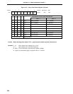
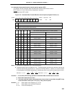
Data Transfer Interval Specification (f
XX
= 5.0 MHz Operation)
ADTI4 ADTI3 ADTI2 ADTI1
0
0
0
0
0
0
0
0
0
0
0
0
0
0
0
0
0
0
0
0
0
0
0
0
1
1
1
1
1
1
1
1
0
0
0
0
1
1
1
1
0
0
0
0
1
1
1
1
0
0
1
1
0
0
1
1
0
0
1
1
0
0
1
1
Minimum
Note 2
18.4
s + 0.5/f
SCK
31.2
s + 0.5/f
SCK
44.0
s + 0.5/f
SCK
56.8
s + 0.5/f
SCK
69.6
s + 0.5/f
SCK
82.4
s + 0.5/f
SCK
95.2
s + 0.5/f
SCK
108.0
s + 0.5/f
SCK
120.8
s + 0.5/f
SCK
133.6
s + 0.5/f
SCK
146.4
s + 0.5/f
SCK
159.2
s + 0.5/f
SCK
172.0
s + 0.5/f
SCK
184.8
s + 0.5/f
SCK
197.6
s + 0.5/f
SCK
210.4
s + 0.5/f
SCK
Maximum
Note 2
20.0
s + 1.5/f
SCK
32.8
s + 1.5/f
SCK
45.6
s + 1.5/f
SCK
58.4
s + 1.5/f
SCK
71.2
s + 1.5/f
SCK
84.0
s + 1.5/f
SCK
96.8
s + 1.5/f
SCK
109.6
s + 1.5/f
SCK
122.4
s + 1.5/f
SCK
135.2
s + 1.5/f
SCK
148.0
s + 1.5/f
SCK
160.8
s + 1.5/f
SCK
173.6
s + 1.5/f
SCK
186.4
s + 1.5/f
SCK
199.2
s + 1.5/f
SCK
212.0
s + 1.5/f
SCK
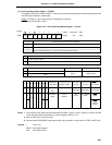
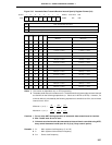
65432107
Symbol
ADTI ADTI7 0 0 ADTI4 ADTI3 ADTI2 ADTI1 ADTI0
FF6BH 00H R/W
Address After Reset R/W
ADTI7
0
Data Transfer Interval Control
No control of interval by ADTI
Note 1
Control of interval by ADTI (ADTI0 to ADTI4) 1
ADTI0
0
1
0
1
0
1
0
1
0
1
0
1
0
1
0
1
µ
µ
µ
µ
µ
µ
µ
µ
µ
µ
µ
µ
µ
µ
µ
µ
µ
µ
µ
µ
µ
µ
µ
µ
µ
µ
µ
µ
µ
µ
µ
µ
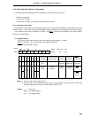
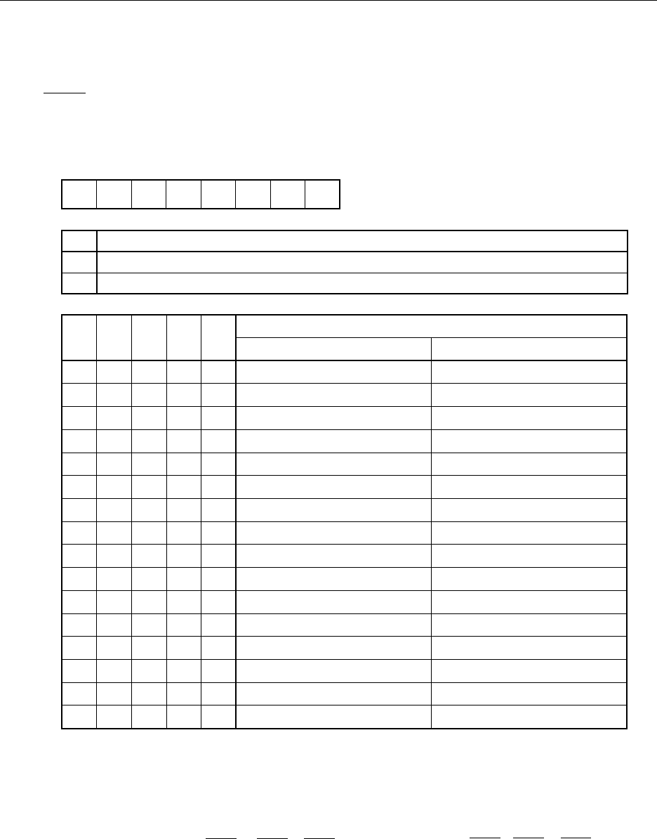
(4) Automatic data transmit/receive interval specify register (ADTI)
This register sets the automatic data transmit/receive function data transfer interval.
ADTI is set by a 1-bit or 8-bit memory manipulation instruction.
RESET input sets ADTI to 00H.
Figure 18-5. Automatic Data Transmit/Receive Interval Specify Register Format (1/4)
Notes 1. The interval is dependent only on CPU processing.
2. The data transfer interval includes an error. The data transfer minimum and maximum intervals are
found from the following expressions (n: Value set in ADTI0 to ADTI4). However, if a minimum which
is calculated by the following expressions is smaller than 2/f
SCK, the minimum interval time is 2/fSCK.
Minimum = (n+1) × + + , Maximum = (n+1) × + +
Cautions 1. Do not write ADTI during operation of automatic data transmit/receive function.
2. Bits 5 and 6 must be set to zero.
3. If the auto send and receive data transmission interval time is controlled using ADTI, busy
control becomes invalid (see 18.4.3 (4) (a) Busy control option).
Remarks 1. f
XX : Main system clock frequency (fX or fX/2)
2. fX : Main system clock oscillation frequency
3. fSCK : Serial clock frequency
2
6
28 0.5
f
XX fXX fSCK
2
6
fXX
36
f
XX
1.5
f
SCK