


540
CHAPTER 26
µ
PD78P058F, 78P058FY
Program inhibit High impedance
26.3 PROM Programming
The
µ
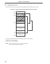
PD78P058F and 78P058FY include on-chip PROM in a 60 Kbyte configuration as program memory. To
write a program into the
µ
PD78P058F or 78P058FY PROM, make the device enter the PROM programming
mode by setting the levels of the VPP and RESET pins as specified. For the connection of unused pins, see
paragraph (2) PROM programming mode in section 1.5 or 2.5 Pin Configuration (Top View).
Caution Write the program in the range of addresses 0000H to EFFFH (specify the last address as
EFFFH.) The program cannot be correctly written by a PROM programmer which does not have
a write address specification function.
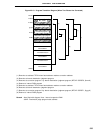
26.3.1 Operating modes
When +5 V or +12.5 V is applied to the V
PP pin and a low-level signal is applied to the RESET pin, the
µ
PD78P058F
and
µ
PD78P058FY are set to the PROM programming mode. This is one of the operating modes shown in Table
26-4 below according to the setting of the CE, OE, and PGM pins.
The PROM contents can be read by setting the read mode.
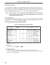
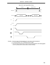
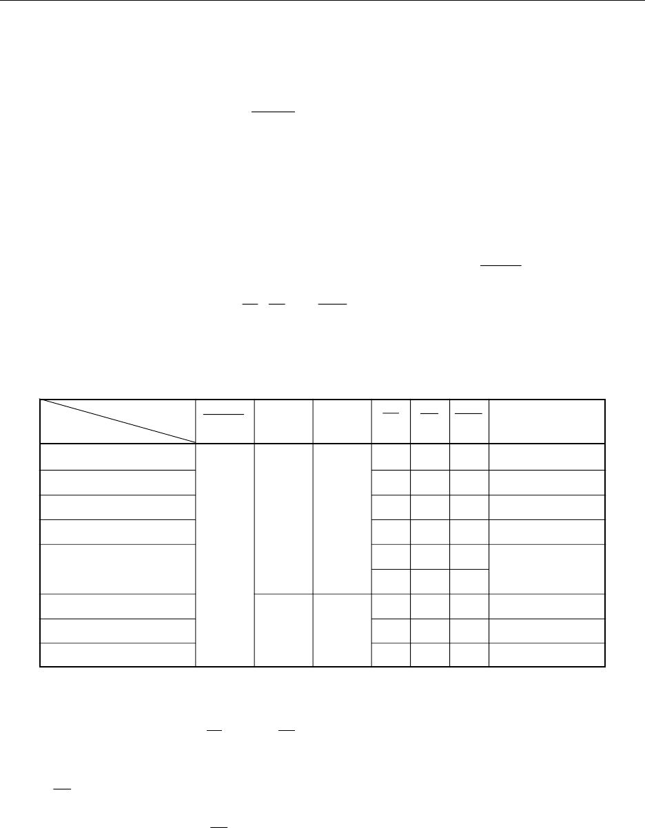
Table 26-4. PROM Programming Operating Modes
Pin
Operating Mode
Page data latch H L H Data input
Page write H H L High impedance
Byte write L H L Data input
Program verify L L H Data output
L × HH
× LL
Read L L H Data output
Output disabled +5 V +5V L H × High impedance
Standby H ××High impedance
Remark ×: L or H
(1) Read mode
Read mode is set by setting CE to L and OE to L.
(2) Output disable mode
If OE is set to H, data output becomes high impedance and the output disable mode is set.
Therefore, if multiple
µ
PD78P058Fs or 78P058FYs are connected to the data bus, data can be read from any
one device by controlling the OE pin.
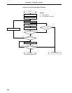
RESET V
PP VDD CE OE PGM D0 to D7
+12.5 V +6.5 V