


323
CHAPTER 16 SERIAL INTERFACE CHANNEL 0 (
µ
PD78058F SUBSERIES)
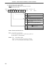
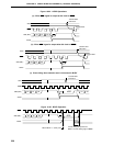
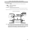
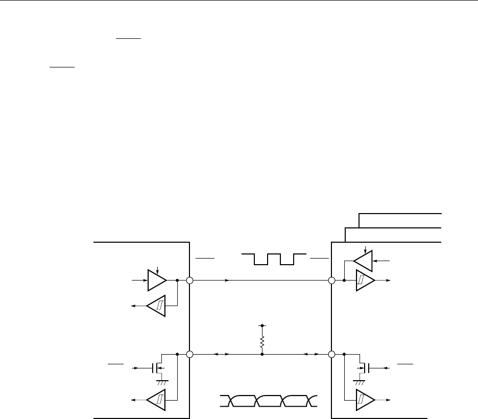
(5) Pin configuration
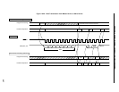
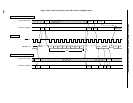
The serial clock pin SCK0 and serial data bus pin SB0 (SB1) have the following configurations.
(a) SCK0 ............ Serial clock input/output pin
<1> Master.. CMOS and push-pull output
<2> Slave .... Schmitt input
(b) SB0 (SB1) .... Serial data input/output dual-function pin
Both master and slave devices have an N-ch open drain output and a Schmitt input.
Because the serial data bus line has an N-ch open-drain output, an external pull-up resistor is necessary.
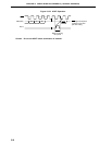
Figure 16-26. Pin Configuration
Caution When receiving data, it is necessary to set the N-ch open drain output in the high impedance
state, so please write FFH in serial I/O shift register 0 (SIO0) in advance. This will keep it
in the high impedance state at all times during transmission. However, in the case of the
wake up function instruction bit (WUP) = 1, the N-ch open drain output is always in the high
impedance state, so it is not necessary to write FFH in SIO0 before reception.
SI0
SO0
SI0
SO0
(Clock Input)
Clock Output
Master Device
Clock Input
(Clock Output)
Serial Clock
SCK0
SCK0
R
L
Serial Data Bus
SB0 (SB1) SB0 (SB1)
N-ch Open-Drain N-ch Open-Drain
Slave Device
AV
DD
AV
SS
AV
SS