


351
CHAPTER 17 SERIAL INTERFACE CHANNEL 0 (
µ
PD78058FY SUBSERIES)
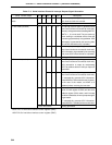
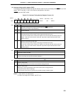
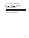
(4) Interrupt timing specify register (SINT)
This register sets the bus release interrupt and address mask functions and displays the SCK0/SCL pin level
status. SINT is set with a 1-bit or 8-bit memory manipulation instruction.
RESET input sets SINT to 00H.
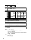
Figure 17-6. Interrupt Timing Specify Register Format (1/2)
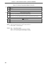
Notes 1. Bit 6 (CLD) is a read-only bit.
2. When not using the I
2
C mode, set CLC to 0.
Used in I
2
C bus mode.
Make SCL pin enter high-impedance state unless serial transfer is being performed.
(except for clock line which is kept high)
Used to enable master device to generate start condition and stop condition signals.
65432107
Symbol
SINT 0 CLD SIC SVAM CLC WREL WAT1 WAT0
FF63H 00H R/W
Note 1
Address After Reset R/W
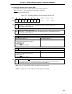
WREL
0
Wait state has been cancelled.
Cancels wait state. Automatically cleared to 0 when the state is cancelled.
(Used to cancel wait state by means of WAT0 and WAT1.)
CLC
0
1
Clock Level Control
Note 2
Used in I
2
C bus mode.
Make output level of SCL pin low unless serial transfer is being performed.
R/W
1
Wait Sate Cancellation Control
R/W
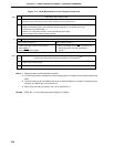
WAT1
0
1
Wait and Interrupt Control
Generates interrupt service request at rising edge of 8th SCK0 clock cycle.
(keeping clock output in high impedance)
R/W
WAT0
0
0
Used in I
2
C bus mode. (8-clock wait)
Generates interrupt service request at rising edge of 8th SCK0 clock cycle.
(In the case of master device, makes SCL output low to enter wait state after 8 clock pulses are
output. In the case of slave device, makes SCL output low to request wait state after 8 clock
pulses are input.)
1
1
Used in I
2
C bus mode. (9-clock wait)
Generates interrupt service request at rising edge of 9th SCK0 clock cycle.
(In the case of master device, makes SCL output low to enter wait state after 9 clock pulses are
output. In the case of slave device, makes SCL output low to request wait state after 9 clock
pulses are input.)
0 Setting prohibited
1