180 AMD Geode™ LX Processors Data Book
CPU Core Register Descriptions
33234H
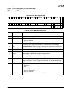
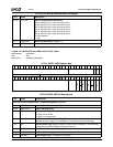
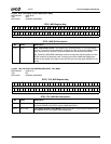
5.5.2.86 L2 TLB/DTE/PTE Entry MSR (L2TLB_ENTRY_MSR)
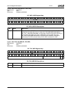
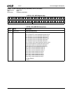
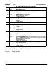
21:16 PTE_LRU 4M PTE Least Recently Used Value.
Bit 21: 4M PTE entry 0 more recent than entry 1.
Bit 20: 4M PTE entry 0 more recent than entry 2.
Bit 19: 4M PTE entry 0 more recent than entry 3.
Bit 18: 4M PTE entry 1 more recent than entry 2.
Bit 17: 4M PTE entry 1 more recent than entry 3.
Bit 16: 4M PTE entry 2 more recent than entry 3.
0: False (Default)
1: True
15:1 RSVD (RO) Reserved (Read Only). (Default = 0)
0 L2WR1 L2 Write to Way 1. Next L2 TLB write to way 1 if both ways are valid. (Default = 0)
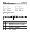
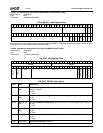
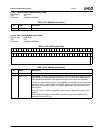
MSR Address 0000189Eh
Typ e R /W
Reset Value 00000000_00000000h
L2TLB_LRU_MSR Bit Descriptions (Continued)
Bits Name Description
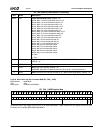
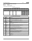
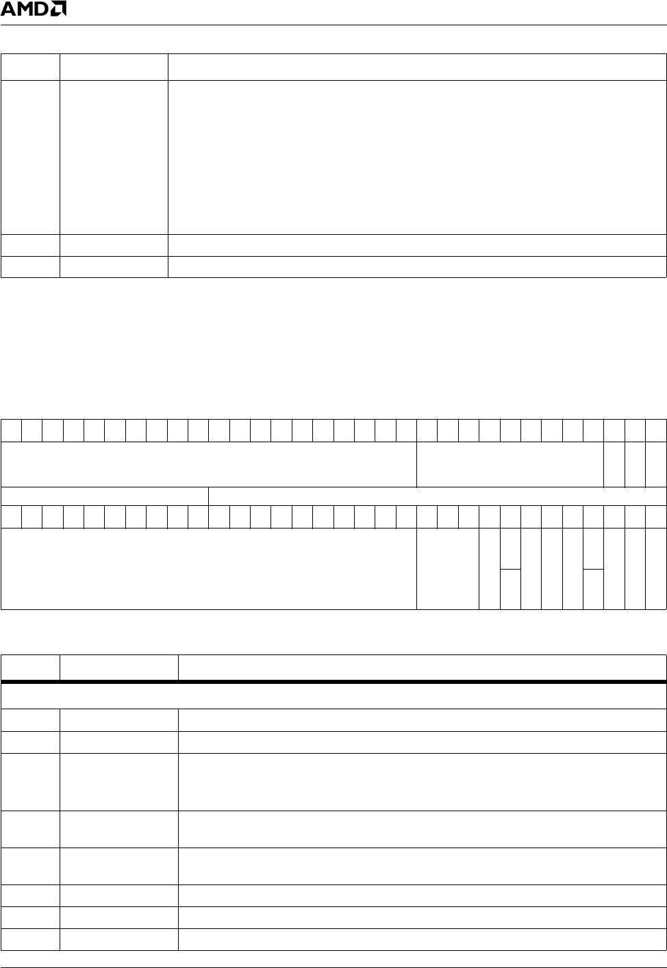
L2TLB_ENTRY_MSR Register Map
63 62 61 60 59 58 57 56 55 54 53 52 51 50 49 48 47 46 45 44 43 42 41 40 39 38 37 36 35 34 33 32
LINADDR RSVD
WP
WA_WS
WC
LINADDR RSVD
313029282726252423222120191817161514131211109876543210
PHYSADDR RSVD
GLOBAL
RSVD
DIRTY
ACC
CD
WT_BR
US
WR
VALID
4MPTE
WT
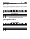
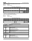
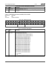
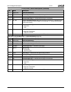
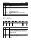
L2TLB_ENTRY_MSR Bit Descriptions
Bit Name Description
If SEL bits in L2TLB_INDEX MSR = 0x (MSR 0000189Ch[17:16] = 0x)
63:44 LINADDR Linear Address. Address [32:12].
43:35 RSVD (RO) Reserved (Read Only).
34 WP Write-protect Flag.
0: Page can be written.
1: Page is write-protected.
33 WA_WS Write-allocate/Write-serialize Flag. If the page is cacheable, a 1 indicates the write-
allocate flag. If the page is non-cacheable, a 1 indicates the write-serialize flag.
32 WC Write-combine Flag. When this page is marked as non-cacheable, a 1indicates that
writes may be combined before being sent to the bus.
31:12 PHYSADDR Physical Address. Address [32:12]
11:9 RSVD (RO) Reserved (Read Only).
8 GLOBAL Global Page Flag. A 1 indicates a global page.


