AMD Geode™ LX Processors Data Book 497
Video Input Port Register Descriptions
33234H
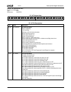
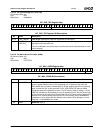
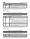
6.10.2.9 VIP Task A VBI Even Base Address (VIP_TASK_A_VBI_EVEN_BASE)
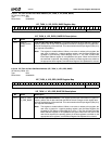
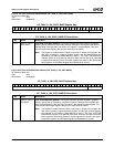
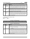
6.10.2.10 VIP Task A VBI Odd Base Address (VIP_TASK_A_VBI_ODD_BASE)
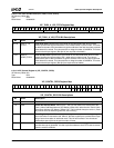
VIP Memory Offset 20h
Typ e R /W
Reset Value 00000000h
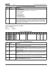
VIP_TASK_A_VBI_EVEN_BASE Register Map
31 30 29 28 27 26 25 24 23 22 21 20 19 18 17 16 15 14 13 12 11 10 9 8 7 6 5 4 3 2 1 0
TASK_A_VBI_DATA_EVEN_BASE Program to 00000
VIP_TASK_A_VBI_EVEN_BASE Bit Descriptions
Bit Name Description
31:0 TASK_A_VBI_E
VEN_BASE
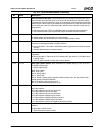
Task AVBI Even Base Address. This register specifies the base address in graphics
memory where VBI data for even fields is stored. Changes to this register take effect at
the beginning of the next field. The value in this register is 16-byte aligned. This value
needs to be 32-byte aligned. (Bits [4:0] are required to be 00000.)
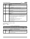
Note: This register is double buffered. When a new value is written to this register, the
new value is placed in a special pending register, and the Base Register Not
Updated bit (VIP Memory Offset 08h[16]) is set to 1. The Task A VBI Even Base
Address register is not updated at this point. When the first data of the next field
is captured, the pending values of all base registers are written to the appropriate
base registers, and the Base Register Not Updated bit is cleared.
VIP Memory Offset 24h
Typ e R /W
Reset Value 00000000h
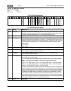
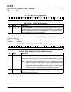
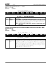
VIP_TASK_A_VBI_ODD_BASE Register Map
313029282726252423222120191817161514131211109876543210
TASK_A_VBI_DATA_ODD_BASE Program to 00000
VIP_TASK_A_VBI_ODD_BASE Bit Description
Bit Name Description
31:0 TASK_A_VBI_O
DD_BASE
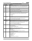
Task A VBI Odd Base Address. This register specifies the base address in graphics
memory where Task A VBI data for odd fields are stored. Changes to this register take
effect at the beginning of the next field. The value in this register is 8-byte aligned. This
value needs to be 32-byte aligned. (Bits [4:0] are required to be 00000.)
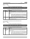
Note: This register is double buffered. When a new value is written to this register, the
new value is placed in a special pending register, and the Task A Base Register
Not Updated bit (VIP Memory Offset 08h[16]) is set to 1. The Task A VBI Odd
Base Address register is not updated at this point. When the first data of the next
field is captured, the pending values of all base registers are written to the appro-
priate base registers, and the Base Register Not Updated bit is cleared.


