AMD Geode™ LX Processors Data Book 457
Video Processor Register Descriptions
33234H
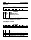
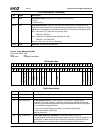
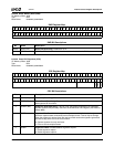
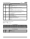
6.8.3.47 Dither RAM Control and Address (DCA)
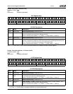
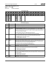
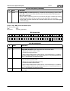
0DENB Dithering Enable. Enable/disable dithering. The dither bit must be enabled in order for dither
RAM reads or writes to occur. When this bit is cleared, the internal dither RAM is powered
down, which saves power.
0: Dither disable. The dithering function is turned off. When the dither is disabled the Dithering
Bits Select (bits [3:1]) do not have any effect and the dither RAM is not accessible.
1: Dither enable. The dither functions with the number of dither bits as set in the Dithering Bits
Select (bits [3:1]).
VP Memory Offset 448h
Typ e R /W
Reset Value 00000000_00000000h
DFC Bit Descriptions (Continued)
Bit Name Description
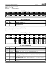
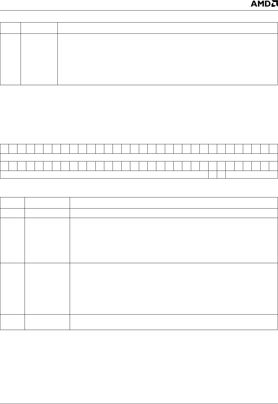
DCA Register Map
63 62 61 60 59 58 57 56 55 54 53 52 51 50 49 48 47 46 45 44 43 42 41 40 39 38 37 36 35 34 33 32
RSVD
313029282726252423222120191817161514131211109876543210
RSVD A U ADDR
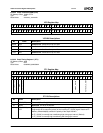
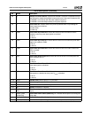
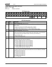
DCA Bit Descriptions
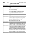
Bit Name Description
63:8 RSVD (RO) Reserved (Read Only). Reads back as 0.
7A Dither RAM Access Bit. Allows reads and writes to/from Dither RAM.
0: Disable (do not allow reads or writes).
1: Enable (allow reads and writes).
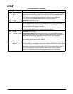
To perform dither RAM writes and reads, both bits 7 and 6 must be set to 1. In addition
VP Memory Offset 418h bits 12 and 0 must both be set to 1. If any of these bits are not
set to 1, the RAM goes into power-down mode.
6U Dither RAM Update. This bit works in conjunction with bit 7. If this bit is enabled, it
allows the data to update the RAM.
0: Disable (do not allow dither RAM accesses).
1: Enable (allow dither RAM accesses).
To perform dither RAM writes and reads, both bits 7 and 6 must be set to 1. In addition
VP Memory Offset 418h bits 12 and 0 must both be set to 1. If any of these bits are not
set to 1, the RAM goes into power-down mode.
5:0 ADDR RAM Address. This 6-bit field specifies the address to be used for the next access to the
dither RAM.


