AMD Geode™ LX Processors Data Book 351
Display Controller Register Descriptions
33234H
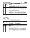
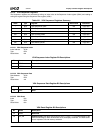
6.6.14 Even Field Video Address Registers
6.6.14.1 DC Even Field Video Y Start Address Offset (DC_VID_EVEN_Y_ST_OFFSET)
Settings written to this register do not take effect until the start of the next even interlaced field.
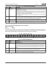
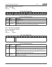
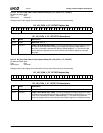
20 VIP_VSYNC_
WAIT (RO)
VIP VSYNC Wait (Read Only). If set to 1 this status bit indicates that the DC has com-
pleted a field or frame and is waiting for the VIP’s VSYNC to go active before beginning
another frame. Typically, this will occur only if the VIP_VIDEO_OK (bit 23) input is active
or the GENLOCK_TO _EN (bit 19) is inactive.
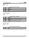
19 GENLK_TO_EN GenLock Time Out Enable. Setting this bit allows the DC to revert to its own internal
timer if a loss of sync is detected by the VIP. This allows for seamless operation of the
DC in GenLock mode when the VIP input becomes unstable. Clearing this bit forces the
DC to wait for a VSYNC signal from the VIP even if the VIP indicates a loss of sync.
18 GENLK_EN GenLock Enable. When set to 1, the DC resets to the start of the frame/field upon
receipt of a rising edge on the VIP_VSYNC signal.
17:0 GENLK_SKW GenLock Skew. This value indicates how many Dot clocks to delay the internal recogni-
tion of the VIP VSYNC by the DC when GenLock is enabled. If GenLock timeout is also
enabled (GENLK_TO_EN, bit 19 = 1), internal recognition of VSYNC occurs immediately
upon timeout (without allowing this skew time to elapse after the timeout is detected.)
This allows seamless transition from a VIP-supplied VSYNC to an internally-determined
VSYNC, while still allowing for a delay in timeout detection.
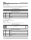
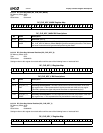
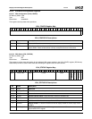
DC Memory Offset 0D8h
Typ e R /W
Reset Value xxxxxxxxh
DC_GENLK_CTL Bit Descriptions (Continued)
Bit Name Description
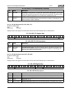
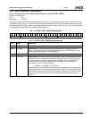
DC_VID_EVEN_Y_ST_OFFSET Register Map
313029282726252423222120191817161514131211109876543210
RSVD OFFSET
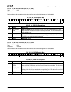
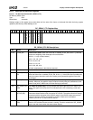
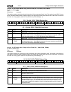
DC_VID_EVEN_Y_ST_OFFSET Bit Descriptions
Bit Name Description
31:28 RSVD Reserved. Set to 0.
27:0 OFFSET Video Y Even Buffer Start Offset. This value represents the starting location for Video
Y Buffer for even fields when interlacing is enabled. This field is not used when interlac-
ing is disabled (DC Memory Offset 094h[11] = 0).
This value represents the starting location for Video Y Buffer for even fields when inter-
lacing is enabled (DC Memory Offset 094h[11] = 1). The lower five bits should always be
programmed as zero so that the start offset is aligned to a 32-byte boundary. If YUV
4:2:2 mode is selected (DC Memory Offset 004h[20] = 0), the Video Y Buffer is used as a
singular buffer holding interleaved Y, U and V data. If YUV 4:2:0 is selected (DC Memory
Offset 004h[20] = 1), the Video Y Buffer is used to hold only Y data while U and V data
are stored in separate buffers.


