AMD Geode™ LX Processors Data Book 297
Display Controller
33234H
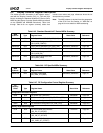
6.5.9 Interlaced Modes
For interlaced modes, the V_ACTIVE and V_TOTAL fields
are configured for the odd field. The Even Field Vertical
Timing registers (DC Memory Offsets 0E4h-0ECh) are
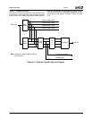
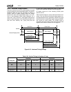
configured for the corresponding even field. Figure 6-22 on
page 298 shows a representative timing diagram for the
odd and even timing register settings in interlaced modes,
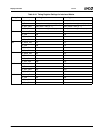
and Table 6-43 on page 298 presents the (decimal) timing
values for some common interlaced modes.
The DC is capable of producing an interlaced output using
any of three separate mechanisms. It can fetch the graph-
ics data in an interlaced manner, flicker filter the graphics
data, or use the same graphics data for both odd and even
fields, (which would effectively line-double the resulting
image). When the VGA is being used, interlaced address-
ing is not supported, and scaling must be used. When the
frame buffer source image or the output image is wider
than 1024 active pixels, the flicker filter is not supported.
When scaling and/or interleaving is enabled, the size of the
frame buffer image (in pixels) will vary from the size of the
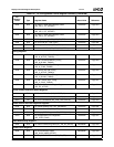
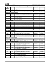
output image. Table 6-42 and Table 6-44 on page 299 indi-
cates how the DC’s timing register fields should be pro-
grammed for supported scaling and interlacing modes.
(Note that for VGA modes, there are several VGA registers
that can affect the size of the frame buffer image. These
registers are not enumerated in the table.)
Table 6-42. Programming Image Sizes
Mode
Pre-scale
Horizontal
Width
Pre-scale
Height
Post-scaler
Width
Post-scaler
Height
Final (Output)
Width
Final (Output)
Height
Default (no VGA, scal-
ing, interlacing, or flicker
filter)
H_ACTIVE V_ACTIVE H_ACTIVE V_ACTIVE H_ACTIVE V_ACTIVE
Scaling only FB_H_ACTIVE FB_V_ACTIVE H_ACTIVE V_ACTIVE H_ACTIVE V_ACTIVE
Interlacing only (no flicker
filter)
H_ACTIVE V_ACTIVE or
V_ACTIVE_EVE
N (alternating)
H_ACTIVE V_ACTIVE or
V_ACTIVE_EVE
N (alternating)
H_ACTIVE V_ACTIVE or
V_ACTIVE_EVE
N (alternating)
Interlacing with flicker fil-
ter
H_ACTIVE V_ACTIVE +
V_ACTIVE_EVE
N + 1 (Note 1)
H_ACTIVE V_ACTIVE +
V_ACTIVE_EVE
N + 11
H_ACTIVE V_ACTIVE or
V_ACTIVE_EVE
N (alternating)
Interlacing with inter-
laced addressing (no
flicker filter)
H_ACTIVE V_ACTIVE or
V_ACTIVE_EVE
N (alternating)
H_ACTIVE V_ACTIVE or
V_ACTIVE_EVE
N (alternating)
H_ACTIVE V_ACTIVE or
V_ACTIVE_EVE
N (alternating)
Interlacing with scaler (no
flicker filter, no interlaced
addressing)
FB_H_ACTIVE FB_V_ACTIVE H_ACTIVE V_ACTIVE or
V_ACTIVE_EVE
N (alternating)
H_ACTIVE V_ACTIVE or
V_ACTIVE_EVE
N (alternating)
Interlacing with scaler
and flicker filter
FB_H_ACTIVE FB_V_ACTIVE H_ACTIVE V_ACTIVE +
V_ACTIVE_EVE
N + 11
H_ACTIVE V_ACTIVE or
V_ACTIVE_EVE
N (alternating)
VGA (no scaling, interlac-
ing, or flicker filter)
VGA CRTC VGA CRTC VGA CRTC VGA CRTC VGA CRTC VGA CRTC
VGA with scaling (no
interlacing or flicker filter
VGA CRTC VGA CRTC H_ACTIVE V_ACTIVE H_ACTIVE V_ACTIVE
VGA with scaling and
interlacing (no flicker fil-
ter)
VGA CRTC VGA CRTC H_ACTIVE V_ACTIVE or
V_ACTIVE_EVE
N (alternating)
H_ACTIVE V_ACTIVE or
V_ACTIVE_EVE
N (alternating)
VGA with scaling, inter-
lacing, and flicker filter
VGA CRTC VGA CRTC H_ACTIVE V_ACTIVE +
V_ACTIVE_EVE
N + 11
H_ACTIVE V_ACTIVE or
V_ACTIVE_EVE
N (alternating)
Note 1. Because the register value represents the image size minus 1, an additional 1 is added when these two register values are added
together to retain the convention.


