AMD Geode™ LX Processors Data Book 555
GeodeLink™ Control Processor Register Descriptions
33234H
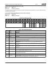
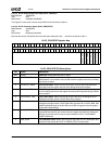
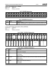
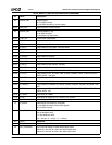
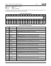
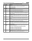
23:16 HOLD_COUNT Hold Count. The number of PLL reference clock cycles (divided by 16) that the PLL is
powered down for, and also the number before releasing CHIP_RESET.
0: Wait 0 cycles. (Default)
1: Wait 16 clock cycles, etc.
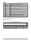
15 RSVD Reserved. Always write 0.
14 GLIUPD GLIU Power Down. This signal controls the power down mode of the GLIU PLL. It is
active high. This bit is always cleared by a CHIP_RESET (bit 0).
13 COREPD Core Power Down. This signal controls the power down mode of the CPU core PLL. It is
active high. This bit is always cleared by a CHIP_RESET (bit 0).
12 GLIUBYPASS GLIU Bypass. This signal controls the Bypass mode of the GLIU clocking. If this bit is
high, the DOTPLL is configured for bypass and the DOTREF input clock directly drives
the GLIU clock spines. (For SYSREF bypass through the GLIU PLL, the CLKSEL JTAG
register must be used).
11 COREBYPASS Core Bypass. This signal controls the Bypass mode of the Core clock. If this bit is high,
the DOTPLL is configured for bypass and the DOTREFF input clock directly drives the
Core clock. (For SYSREF bypass through the Core PLL, the CLKSEL JTAG register
must be used).
10 LPFEN Loop Filter Enable. This bit is tied to both the GLIU and Core PLL loop filter enables.
This PLL control enables the use of an external resistor. It should be clear for normal
operation.
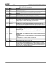
9 VA_SEMI_
SYNC_MODE
CPU Sync Mode. This bit controls whether the CPU uses a FIFO for interfacing with the
GLIU. If the bit is high, the CPU will not use the FIFO. It behaves as if the CPU and GLIU
domains are synchronous. This bit can be set high as long as the CPU and GLIU fre-
quencies are multiples of each other. The bit is always reset low.
8 PCI_SEMI_
SYNC_MODE
PCI Sync Mode. This bit controls whether the PCI uses the falling edges of mb_func_clk
and pci_func_clk for interfacing with GLIU or not. If the bit is high, PCI does not use fall-
ing clock edges. It behaves as if the PCI and GLIU domains are synchronous. This bit
can be set high as long as the PCI and GLIU frequencies are multiples of each other. The
bit always resets low.
7:1 BOOTSTRAPS
(RO)
Bootstraps (Read Only). These bits are copies of the state of bootstraps when power-
on reset (PCI reset) is released.
Bit 7: PW1 pad - active high when the PCI clock is 66 MHz, low for 33 MHz.
Bit 6: IRQ13 pad - active high for stall-on-reset debug feature, otherwise low.
Bit 5: PW0 pad - part of CPU/GLIU frequency selects.
Bit 4: SUSPA# pad - part of CPU/GLIU frequency selects.
Bit 3: GNT2# pad - part of CPU/GLIU frequency selects.
Bit 2: GNT1# pad - part of CPU/GLIU frequency selects.
Bit 1: GNT0# pad - part of CPU/GLIU frequency selects.
0 CHIP_RESET Chip Reset. When written to a 1, the chip enters reset and does not come out until the
HOLD_COUNT (bits [23:16]) is reached. This register and the JTAG logic are not reset
by CHIP_RESET, but otherwise the entire chip is reset. (Default = 0)
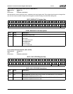
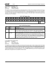
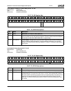
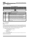
GLCP_SYS_RSTPLL Bit Descriptions (Continued)
Bit Name Description


