298 AMD Geode™ LX Processors Data Book
Display Controller
33234H
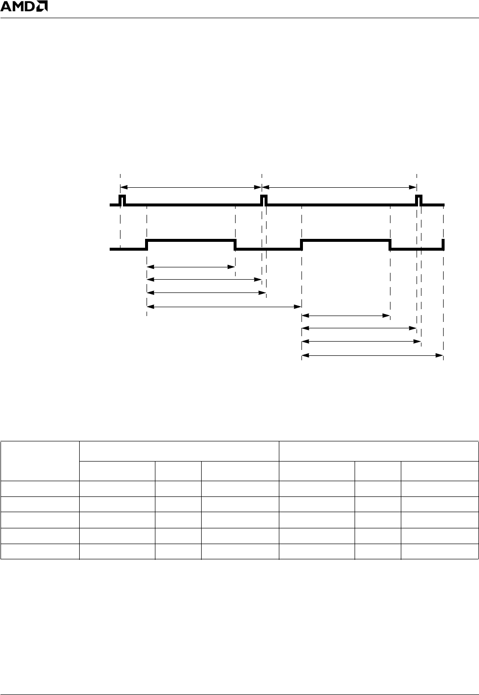
6.5.10 Interlaced Timing Examples
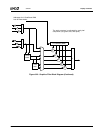
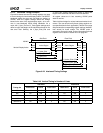
Figure 6-22 shows how the DC's timing registers are used
to control timings for interlaced display modes. The SMTPE
standards define the even and odd fields as starting at
VSYNC, while the register settings define the timings
based on the start of the active display region, as is com-
mon in (non-interlaced) VESA timing standards. As a
result, the V_Sync_End and V_Total register settings each
define a region that begins in the odd field and ends in the
next even field. Similarly, the V_Sync_Even_End and
V_Total_Even register settings each define a region that
begins in the even field and ends in the next odd field.
All register values are in hex; assuming VSYNC pulse
width of one line.
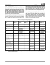
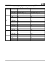
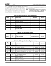
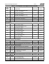
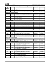
Table 6-43 lists timings for various interlaced modes for ref-
erence. The user should verify these timings against cur-
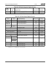
rent specifications for their application.) Table 6-44 on page
299 provides the corresponding register settings (hexadec-
imal values) for these modes. The VSYNC pulse is
assumed to be one line wide. Further information on these
registers can be found in Section 6.6.5 on page 327.
Figure 6-22. Interlaced Timing Settings
.
VSYNC
Vertical Display Active
Odd Field Even Field
Back
Porch
Front
Porch
Back
Porch
Front
Porch
Active Region Active Region
V_Active_End
V_Total
V_Sync_Start
V_Sync_End
V_Active_Even_End
V_Total_Even
V_Sync_Even_Start
V_Sync_Even_End
Back
Porch
Table 6-43. Vertical Timing in Number of Lines
Timing Set
Odd Field Even Field
Back Porch Active Front Porch Back Porch Active Front Porch
525 16 242 2 17 241 3
625 22 288 2 23 288 2
720i 12 360 3 13 360 2
1080i 20 540 3 20 540 2
1080i 50 Hz 80 540 5 80 540 5


