AMD Geode™ LX Processors Data Book 535
GeodeLink™ Control Processor
33234H
EXTEST JTAG Instruction
The EXTEST instruction accesses the boundary scan
chain around the chip and controls the pin logic such that
the boundary scan data controls the data and enable sig-
nals for the pins. IEEE 1149.1 requires that an all-zero
instruction access the boundary scan chain; the controller
actually catches the all-zero condition during the “Update-
IR” state and loads 1FFFFE8h into the internal instruction
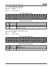
register. As seen by Table 6-82, this select OP = 000
(access boundary scan chain) and selectJtagOut# is set
active so that the boundary cells control the pads.
DELAY_CONTROLS
This chain controls the delay timing for the inputs and out-
puts. This register can be overridden with an MSR write to
GLCP_DELAY_CONTROLS (GLCP MSR 4C00000Fh) if
bit 63 of the MSR is set high. Bits [62:0] of this register
have the same meaning as in the MSR description for
GLCP_DELAY_CONTROLS (see Section 6.14.2.8 on page
549).
REVID
This 8-bit JTAG register can be reprogrammed with any
metal layer change to identify silicon changes. This register
has the same value as the GLCP REV_ID bits (MSR
4C002000h[7:0]).
MULTISCAN
During manufacturing test, multiple scan chains are avail-
able on the signal pins. Table 6-81 on page 534 identifies
the specific scan behaviors of various pins when in this
mode. The Data register associated with this TAP instruc-
tion is the boundary scan chain and the instruction bits
configure the pads such that the boundary scan ring is pro-
viding data into the core and the captured data on the
boundary scan chain is the data coming from the core.
TRI-STATE
This instruction TRI-STATEs all of the signals. The Data
register accessed is the Bypass register.
BYPASS
According to IEEE 1149.1, shifting all 1s into the IR must
connect the 1-bit Bypass register. The register has no func-
tion except as a storage flip-flop.
6.13.2 Reset Logic
One of the major functions of the GLCP is to control the
resetting of the AMD Geode LX processor. There are two
methods to reset the processor: either by a hard reset
using the input signal RESET#, or by a soft reset by writing
to an internal MSR in the GLCP.
RESET# is used for power-on reset. During power-on
reset, all internal blocks are reset until the release of the
RESET# signal.
Soft reset is activated by writing to GLCP_SYS_RSTPLL
(MSR 4C000014h). Soft reset resets all the internal blocks
to their initial status except the TAP controller. TAP reset is
achieved by holding IRQ13 low during power-on reset.
6.13.3 Clock Control
The clock control function controls the generation of the
AMD Geode LX processor internal clocks. For this pur-
pose, there are two MSRs: GLCP_SYS_RSTPLL and
GLCP_DOTPLL (MSR 4C000014h and 4C000015h).
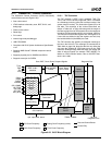
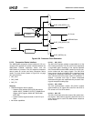
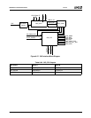
As shown in Figure 6-56 on page 536, the internal clocks
are generated by SYSPLL and DOTPLL. In normal opera-
tion mode MSR 4C000014h[12, 11] = 0 and MSR
4C000015h[15] = 0. The SYSPLL output clock drives the
internal clocks of the CPU Core, the GeodeLink modules,
and SDRAM. The output of DOTPLL drives the DOTCLK,
that in turn, drives the Video Processor and Display Con-
troller modules.
In Bypass mode, when MSR 4C000014h[12] = 1, the DOT-
REF input clock drives the clocks of the GLIU and SDRAM,
and when MSR 4C000014h[11] = 1 the DOTREF input
clock drives the clocks of the CPU Core. Also, when
GLCP_DOTPLL[15] = 1, the DOTREF input drives the
DOTCLK.
6.13.3.1 Power Management
The GLCP controls the chip-wide power management by
controlling when to activate and deactivate the PLL clocks
of the AMD Geode LX processor.
Selection of module-level hardware clock gating is done by
programming the GLD_MSR_PM (MSR 4C002004h) of
each module. When hardware clock gating is activated,
each module enters into power save mode when it is not
busy, and leaves power save mode if a new GeodeLink
request or external event is received.
Each module has a power management module called
clock control.
GLIU1 Power Management Support
The GLCP MSRs directly involved in power management
are:
• GLCP Clock Disable Delay Value
(GLCP_CLK_DIS_DELAY)
• GLCP Global Power Management Controls
(GLCP_GLB_PM)
• GLCP Clock Mask for Sleep Request
(GLCP_PMCLKDISABLE)
• GLCP Clock Active Mask for Suspend Acknowledge
(GLCP_CLK4ACK)
• GLCP Control (GLCP_CNT)
• GLCP Level 2 (GLCP_LVL2)
• GLCP Throttle or C2 Start Delay (GLCP_TH_SD)
• GLCP Scale Factor (GLCP_TH_SF)
• GLCP Processor Throttle Off Delay (GLCP_TH_OD)


