AMD Geode™ LX Processors Data Book 567
GeodeLink™ PCI Bridge
33234H
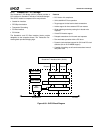
6.15.1 GeodeLink™ Interface Block
The GeodeLink Interface block provides a thin protocol
conversion layer between the Transaction Forwarding block
and GeodeLink Interface Unit 1 (GLIU1). It is responsible
for multiplexing in-bound write request data with out-bound
read response data on the single GLIU1 data out bus.
6.15.2 FIFO/Synchronization Block
The FIFO module consists of a collection of in-bound and
out-bound FIFOs. Each FIFO provides simple, synchro-
nous interfaces to read and write requests.
6.15.3 Transaction Forwarding Block
The Transaction Forwarding block receives, processes, and
forwards transaction requests and responses between the
GeodeLink Interface and PCI Bus Interface blocks. It imple-
ments the transaction ordering rules and performs write
gathering and read prefetching as needed. It also performs
the necessary translation between GLIU1 and PCI com-
mands; except for the creation of PCI configuration cycles
in response to I/O accesses of address 0CFCh. The Trans-
action Forwarding block also handles the conversion
between 64-bit GLIU1 data paths and 32-bit PCI data
paths.
Out-bound transactions are handled in a strongly ordered
fashion. Some out-bound burst writes may be combined
into a larger PCI transaction. This is accomplished by
dynamically concatenating together contiguous bursts as
they are streamed out in a PCI bus transaction. Single 32-
bit WORD accesses are not gathered. It is anticipated that
the processor generates the majority of out-bound
requests. Out-bound memory writes will not be posted.
Thus, any queued out-bound requests need NOT be
flushed prior to handling an in-bound read request.
Dynamic concatenation of contiguous bursts may occur
when reading the penultimate (next to last) data WORD
from the out-bound write data FIFO. On that cycle, if a suit-
able request is available at the head of the out-bound
request FIFO, the PCI burst will be extended.
In-bound requests are handled using slightly relaxed order-
ing. All in-bound writes are gathered as much as possible.
Any partially gathered in-bound writes are flushed when a
cache line boundary is reached. All in-bound writes are
posted. Thus, any queued in-bound write data MUST be
written to system memory prior to the processor receiving
data for an out-bound read request. This is accomplished
by sorting out-bound read response data amongst in-
bound write data. Thus, a pending out-bound read request
need not be deferred while posted in-bound write data is
flushed. The out-bound read request may be performed on
the PCI bus at the same time that the in-bound write data is
flowing through GLIU1.
When handling an in-bound read request, the intended size
of the transfer is unknown. In-bound read requests for non-
prefetchable addresses only fetch the data explicitly indi-
cated in the PCI transaction. Thus, all in-bound read
requests made to non-prefetchable addresses return at
most a single 32-bit WORD. In-bound read requests made
to prefetchable memory may cause more than a 32-bit
WORD to be prefetched. The amount of data prefetched is
configured via the read threshold fields of the CTRL model
specific register of GLPCI_CTRL (MSR 50002010h). Multi-
ple read requests may be generated to satisfy the read
threshold value.
In-bound read requests may pass posted in-bound write
data when there is no address collision between the read
request and the address range of the posted write data (dif-
ferent cache lines) and the read address is marked as
being prefetchable.
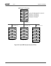
6.15.3.1 Atomic External MSR Access
The companion device implements a mailbox scheme simi-
lar to the AMD Geode LX processor. To access internal
model specific registers on the AMD Geode companion
device’s GLIU it is necessary to perform multiple PCI con-
figuration cycles. The GLPCI module provides a mecha-
nism to give software atomic, transparent access to the
companion device’s GLIU resident MSRs. It translates
MSR read/writes received from the AMD Geode LX pro-
cessor’s GLIUs into the multiple PCI configuration needed
to access the companion device’s internal MSR. From soft-
ware’s point of view, the GLPCI module routes MSR read/
write requests like a GLIU. The GLPCI module terminates
MSR accesses where the three most significant bits are
zero. Otherwise it uses the same three MSBs as an index
to look up a PCI device number and a PCI function number
in GLPCI_EXT (MSR 5000201Eh). This device number is
then further mapped onto AD[31:11] pins using the same
mapping as with software generated PCI configuration
cycles. Next the GLPCI module performs three PCI config-
uration bus cycles.
• Write MSR address to offset F4h
• Read/write MSR data to/from offset F8h
• Read/write MSR data to/from offset FCh
Note: The GLPCI module attempts to do a burst PCI con-
figuration read or write. It is expected that the tar-
get PCI device will typically cause this burst to get
broken up into two by performing a slave termina-
tion after each DWORD of data is transferred.
The GLPCI module can address up to seven external PCI
devices in this manner.


