430 AMD Geode™ LX Processors Data Book
Video Processor Register Descriptions
33234H
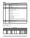
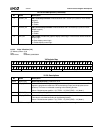
6.8.3.11 Miscellaneous (MISC)
VP Memory Offset 050h
Typ e R /W
Reset Value 00000000_00000C00h
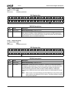
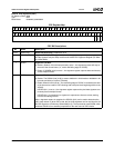
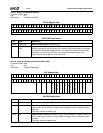
MISC Register Map
63 62 61 60 59 58 57 56 55 54 53 52 51 50 49 48 47 46 45 44 43 42 41 40 39 38 37 36 35 34 33 32
RSVD
313029282726252423222120191817161514131211109876543210
RSVD
SP
APWRDN
DACPWRDN
RSVD
BYP_BOTH
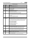
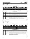
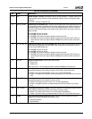
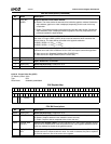
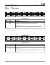
MISC Bit Descriptions
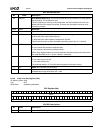
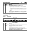
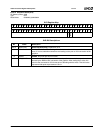
Bit Name Description
63:13 RSVD (RO) Reserved (Read Only). Reads back as 0.
12 SP Spare. Read/write; no function.
11 APWRDN Analog Interface Power Down. Enables power down of the analog section of the inter-
nal CRT DAC.
0: Normal.
1: Power down.
10 DACPWRDN DAC Power Down. Enables power down of the digital section of the internal CRT DAC.
For this bit to take effect:
VP Memory Offset 130h[6] must be = 1 or
MSR Address 48000010h[18:16] must not equal 101.
0: Normal.
1: Power down.
9:1 RSVD (RO) Reserved (Read Only). Reads back as 0.
0 BYP_BOTH Bypass Both. Indicates if both graphics and video data should bypass gamma correc-
tion RAM.
0: The stream selected by the Display Configuration (DCFG) register (VP Memory Offset
008h[21]) is passed through gamma correction RAM.
1: Both graphics and video bypass gamma correction RAM.


