550 AMD Geode™ LX Processors Data Book
GeodeLink™ Control Processor Register Descriptions
33234H
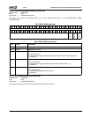
59 SDCLK_SET SDCLK Setup.
0: Full SDCLK setup.
1: Half SDCLK setup for control signals.
58:56 DDR_RLE DDR read latch enable position.
55 SDCLK_DIS SDCLK disable [1,3,5].
0: All SDCLK output.
1: SDCLK[4,2,0] output only.
54:52 TLA1_OA TLA hint pin output adjust.
51:50 D_TLA1 Output delay for TLA1.
49:48 D_TLA0 Output delay for TLA0.
47:46 D_DQ_E Output delay for DQ, DQM - even byte lanes.
45:44 D_DQ_O Output delay for DQ, DQM - odd byte lanes.
43:42 RSVD Reserved.
41:40 D_SDCLK Output delay for SDCLK.
39:38 D_CMD_O Output delay for CKE, CS, RAS, CAS, WE - odd bits.
37:36 D_CMS_E Output delay for CKE, CS, RAS, CAS, WE - even bits.
35:34 D_MA_O Output delay for BA and MA - odd bits.
33:32 D_MA_E Output delay for BA and MA - even bits.
31:30 D_PCI_O Output delay for pci_ad, IRQ13, SUSPA#, INTA# - odd bits.
29:28 D_PCI_E Output delay for pci_ad, CBE#, PAR, STOP#, FRAME#, IRDY#, TRDY#, DEVSEL#,
REQ#, GNT# - even bits.
27:26 D_DOTCLK Output delay for DOTCLK.
25:24 D_DRBG_O Output delay for DRGB[31:0] - odd bits.
23:22 D_DRGB_E Output delay for DRGB[31:0], HSYNC, VSYNC, DISPEN, VDDEN, LDE_MOD - even
bits.
21:20 D_PCI_IN Input delay for AD[31:0], CBE#, PAR, STOP#, FRAME#, IRDY#, TRDY#, DEVSEL#,
REQ#, GNT#, CIS.
19:18 D_TDBGI Input delay for TDBGI.
17:16 D_VIP Input delay for VID[15:0], VIP_HSYNC, VIP_VSYNC.
15:14 D_VIPCLK Input delay for VIPCLK.
13 H_SDCLK Half SDCLK hold select (for cmd addr).
1: Half SDCLK setup for MA and BA signals.
0: Full SDCLK setup.
12:11 PLL_FD_DEL PLL Feedback Delay.
00: No feedback delay.
11: Max feedback delay.
(01: ~350 ps, 10: ~700 ps, 11: ~1100 ps).
10:6 RSVD Reserved.
5 DLL_OV DLL Override (to DLL).
4:0 DLL_OVS/RSDA DLL Override Setting or Read Strobe Delay Adjust.
When DLL Override is 1 this is the DQS overide delay.
When DLL Override is 0 this is the offset adjust value.
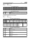
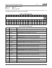
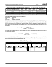
GLCP_DELAY_CONTROLS Bit Definition (Continued)
Bit Name Description


