


21264/EV68A Hardware Reference Manual
Cache and External Interfaces 4–43
Bcache Port
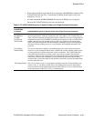
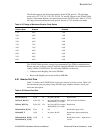
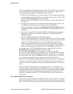
The Bcache supports the following multiples of the GCLK period: 1.5X (dual-data
mode only), 2X, 2.5X, 3X, 3.5X, 4X, 5X, 6X, 7X, and 8X. However, the 21264/EV68A
imposes a maximum Bcache clock period based on the SYSCLK ratio. Table 4–35 lists
the range of maximum Bcache clock periods. Section 4.7.8.2 describes fast mode.
The 21264/EV68A provides a range of programmable Cbox CSRs to manipulate the
Bcache port pins so that a variety of industry-standard SSRAMs can communicate effi-
ciently with the 21264/EV68A. The following SSRAMs can be used:.
• Nonburst mode Reg/Reg late-write SSRAMs
• Burst mode Reg/Reg late-write dual-data SSRAMs
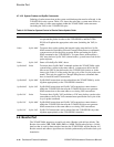
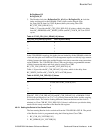
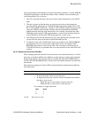
4.8.1 Bcache Port Pins
Table 3–1 defines the 21264/EV68A signal types referred to in this section. Table 4–36
lists the Bcache port pin groups along with their type, number, reference clock, and
functional description.
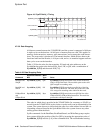
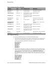
Table 4–35 Range of Maximum Bcache Clock Ratios
SYSCLK Ratio
Bcache Clock Ratio with Fast Mode
Enabled
Bcache Clock Ratio with Fast Mode
Disabled
1.5X 4.0X 7.0X
2.0X 4.0X 7.0X
2.5X 5.0X 8.0X
3.0X 6.0X 8.0X
3.5X 7.0X 8.0X
4.0X 7.0X 8.0X
5.0X 8.0X 8.0X
6.0X 8.0X 8.0X
7.0X 8.0X 8.0X
8.0X 8.0X 8.0X
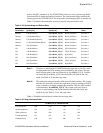
Table 4–36 Bcache Port Pins
Pin Name Type Count Reference Clock Description
BcAdd_H[23:4] O_PP 20 Int_Index_BcClk Bcache index
BcCheck_H[15:0] B_DA_PP 16 Int_Data_BcClk
output
BcDataInClk_H
input
ECC check bits for BcData
BcData_H[127:0] B_DA_PP 128 Int_Data_BcClk
output
BcDataInClk_H
input
Bcache data
BcDataInClk_H[7:0] I_DA 8 NA Bcache data input clocks
BcDataOE_L O_PP 1 Int_Index_BcClk Bcache data output enable/chip
select
BcDataOutClk_H[3:0]
BcDataOutClk_L[3:0]
O_PP 8 NA Bcache data clocks— high and low
version