


3–4 Hardware Interface
21264/EV68A Hardware Reference Manual
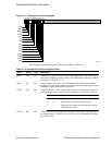
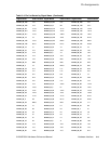
21264/EV68A Signal Names and Functions
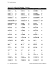
BcDataOutClk_H[3:0]
BcDataOutClk_L[3:0]
O_PP 8 Bcache data output clocks. These free-running clocks are dif-
ferential copies of the Bcache clock and are derived from the
21264/EV68A GCLK. Their period is a multiple of the GCLK
and is fixed for all operations. They can be configured so that
their rising edge lags BcAdd_H[23:4] by 0 to 2 GCLK cycles.
The 21264/EV68A synchronizes tag output information with
these clocks.
BcDataWr_L O_PP 1 Bcache data write enable. The 21264/EV68A asserts this signal
when writing data to the Bcache data arrays.
BcLoad_L O_PP 1 Bcache burst enable.
BcTag_H[42:20] B_DA_PP 23 Bcache tag bits.
BcTagDirty_H B_DA_PP 1 Tag dirty state bit. During cache write operations, the 21264/
EV68A will assert this signal if the Bcache data has been mod-
ified.
BcTagInClk_H I_DA 1 Bcache tag input clock. The 21264/EV68A uses this input
clock to latch the tag information on Bcache read operations.
This clock is used with high-speed SDRAMs, such as DDRs,
that provide a clock-out with data-output pins to optimize
Bcache read bandwidths. The 21264/EV68A internally syn-
chronizes the data to its logic with clock forward receive cir-
cuits similar to the system interface.
BcTagOE_L O_PP 1 Bcache tag output enable. This signal is asserted by the 21264/
EV68A for Bcache read operations.
BcTagOutClk_H
BcTagOutClk_L
O_PP 2 Bcache tag output clock. These clocks “echo” the clock-for-
warded BcDataOutClk_x[3:0] clocks.
BcTagParity_H B_DA_PP 1 Tag parity state bit.
BcTagShared_H B_DA_PP 1 Tag shared state bit. The 21264/EV68A will write a 1 on this
signal line if another agent has a copy of the cache line.
BcTagValid_H B_DA_PP 1 Tag valid state bit. If set, this line indicates that the cache line
is valid.
BcTagWr_L O_PP 1 Tag RAM write enable. The 21264/EV68A asserts this signal
when writing a tag to the Bcache tag arrays.
BcVref I_DC_REF 1 Bcache tag reference voltage.
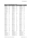
ClkFwdRst_H I_DA 1 Systems assert this synchronous signal to wake up a powered-
down 21264/EV68A. The ClkFwdRst_H signal is clocked
into a 21264/EV68A register by the captured FrameClk_x
signals. Systems must ensure that the timing of this signal
meets 21264/EV68A requirements (see Section 4.7.2).
ClkIn_H
ClkIn_L
I_DA_CLK 2 Differential input signals provided by the system.
DCOK_H I_DA 1 dc voltage OK. Must be deasserted until dc voltage reaches
proper operating level. After that, DCOK_H is asserted.
EV6Clk_H
EV6Clk_L
O_PP_CLK 2 Provides an external test point to measure phase alignment of
the PLL.
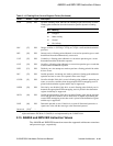
Table 3–2 21264/EV68A Signal Descriptions (Continued)
Signal Type Count Description