21264/EV68A Hardware Reference Manual
Electrical Data 9–9
AC Characteristics
2
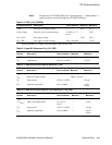
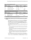
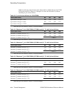
The TDH specified for all clock-forwarded signal groups is with respect to the associated clock.
3
The TSkew value applies only when the SYS_CLK_DELAY[0:1] entry in the Cbox WRITE_ONCE
chain (Table 5–24) is set to zero phases of delay between forwarded clock out and address/data.
4
The TSkew specified for SysData_L signals is only with respect to the associated clock.
5
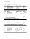
These signals should be referenced to BcTagOutClk_x when measuring TSkew, provided that
BcTagOutClkl_x and BcDataOutClk_x have no programmed offset.
6
The TSkew value applies only when the BC_CLK_DELAY[0:1] entry in the Cbox WRITE_ONCE
chain (Table 5–24) is set to zero phases of delay for Bcache clock.
7
The TSkew specified for BcAdd_H signals is only with respect to the associated clock.
8
The duty cycle for 2.5X single data mode 2 GCLK phases high and 3 GCLK phases low.
9
The duty cycle for 3.5X single data mode 3 GCLK phases high and 4 GCLK phases low.
10
The TSkew specified for BcData_H signals is only with respect to the associated clock pair.
11
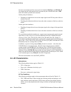
IRQ_H[5:0] must have their TSU and TDH times referenced to DCOK_H during power-up to ensure
the correct Y divider and resulting EV6Clk_x duty cycle. When the 21264/EV68A is executing
instructions IRQ_H[5:0] act as normal asynchronous pins to handle interrupts.
12
Reset_L is an asynchronous pin. It may be asserted asynchronously.
13
DCOK_H is an asynchronous pin. Note the minimum slew rate on the assertion edge.
14
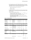
PllBypass_H may not switch when ClkIn_x is running. This pin must either be deasserted during
power-up or the 21264/EV68A core power pin (VDD pins) indicating the 21264/EV68A’s internal
PLL will be used. Note that it is illegal to use PllBypass_H asserted during power-up unless a
ClkIn_x is present.
15
See Section 7.11.2 for a discussion of ClkIn_x as it relates to operating the 21264/EV68A’s internal
PLL versus running the 21264/EV68A in PLL bypass mode. ClkIn_x has specific input jitter require-
ments to ensure optimum performance of the internal 21264/EV68A PLL.
16
In PLL bypass mode, duty cycle deviation from 50%–50% directly degrades device operating fre-
quency.
17
The TSU and TDH of FrameClk_x are referenced to the deasserting edge of ClkIn_x.
18
This signal is a feedback to the internal PLL and may be monitored for overall 21264/EV68A jitter. It
can also be used as a feedback signal to an external PLL when in PLL bypass mode. Proper termina-
tion of EV6Clk_x is imperative.
19
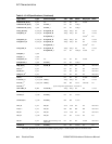
The cycle or phase cannot be more than 5% shorter than the nominal. Do not confuse this measure-
ment with duty cycle.
20
The period for SromClk_H is 256 GCLK cycles.
21
When Trst_L is deasserted, Tms_H must not change state. Trst_L is asserted asynchronously but
may be deasserted synchronously.


