


21264/EV68A Hardware Reference Manual
Electrical Data 9–3
DC Characteristics
Note: Current out of a 21264/EV68A pin is represented by a – symbol while a +
symbol indicates current flowing into a 21264/EV68A pin.
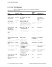
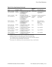
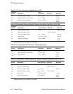
Table 9–3 VDD (I_DC_POWER)
Parameter Symbol Description Test Conditions Minimum Maximum
VDD Processor core supply voltage — 1.6 V 1.7 V
Power (sleep) Processor power required (sleep) @ VDD = 1.7 V
Note 3
—12W
1
1
Power measured at 37.5 MHz while running the “Ebox aliveness test.”
PLL_VDD PLL supply voltage — 2.45 V 2.55 V
PLL_IDD PLL supply current (running) Freq = 940 MHz — 25 mA
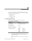
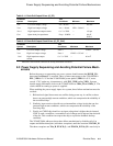
Table 9–4 Input DC Reference Pin (I_DC_REF)
Parameter
Symbol Description Test Conditions Minimum Maximum
VREF DC input reference voltage — 600 mV VDD – 100 mV
|I
I
| Input current VSS ≤ V ≤ VDD — 150 µA
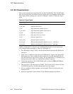
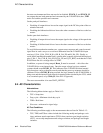
Table 9–5 Input Differential Amplifier Receiver (I_DA)
Parameter
Symbol Description Test Conditions Minimum Maximum
V
IL
Low-level input voltage Note 5 — VREF – 200 mV
V
IH
High-level input voltage — VREF + 200 mV —
|I
I
| Input current VSS ≤ V ≤ VDD — 150 µA
C
IN
Input-pin capacitance Freq =10 MHz — 5.7 pF
Note 6
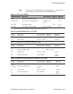
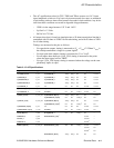
Table 9–6 Input Differential Amplifier Clock Receiver (I_DA_CLK)
Parameter
Symbol Description Test Conditions Minimum Maximum
V
diff
Differential input voltage — 200 mv Note 1 —
| ∆ V
BIAS
| Open-circuit differential I ≤± 1 µA
Note 2
—50mV
|I
I
| Input current VSS ≤ V ≤ VDD — 150 µA
C
IN
Input-pin capacitance Freq =10 MHz — 5.0 pF
Note 6