


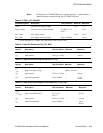

9–6 Electrical Data
21264/EV68A Hardware Reference Manual
AC Characteristics
the tester environment and does not need to be disabled. EV6Clk_L and EV6Clk_H
are outputs that are both generated and consumed by the 21264/EV68A; thus, VDD
tracks for both the producer and consumer.
On the push-pull interfaces:
• Disabling all output drivers leaves the output signal at the DC bias point of the ter-
mination network.
• Disabling the bidirectional drivers leaves the other consumers of the bus as the bus
master.
On the open-drain interfaces:
• Disabling all output drivers leaves the output signal at the voltage of the open-drain
pull-up.
• Disabling all bidirectional drivers leaves the other consumers of the bus as the bus
master.
To avoid failure mechanism number two, systems must sequence and control external
signal flow in such a way as to avoid zero differential into the 21264/EV68A input
receivers (I_DA, I_DA_CLK, B_DA_OD, B_DA_PP, and B_DA_PP). Finally, to
avoid failure mechanism number three, systems must sequence input and bidirectional
pins (I_DA, I_DA_CLK, B_DA_OD, B_DA_PP, and I_DC_REF) such that the 21264/
EV68A does not see a voltage above its VDD.
In addition, as power is being ramped, Reset_L must be asserted — this allows the
21264/EV68A to reset internal state. Once the target voltage levels are attained,
systems should assert DCOK_H. This indicates to the 21264/EV68A that internal
logic functions can be evaluated correctly and that the power-up sequence should be
continued. Prior to DCOK_H being asserted, the logic internal to the 21264/EV68A is
being reset and the internal clock network is running (either clocked by the VCO, which
is at a nominal speed, or by ClkIn_H, if the PLL is bypassed).
The reset state machine is in state WAIT_SETTLE.
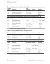
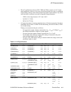
9.4 AC Characteristics
Abbreviations:
The following abbreviations apply to Table 9–13:
• TSU=Setuptime
• Duty cycle = Minimum clock duty cycle
• TDH = Hold time
• Slew rate = referenced to signal edge
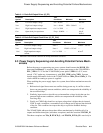
AC Test Conditions:
The following conditions apply to the measurements that are listed in Table 9–13:
• TSU, TDH, and TSkew values include the following onchip and package varia-
tions: min/max metal capacitance, GCLK skew, transistor gate length variation
(OCV), across-chip temperature and voltage variation, and package lead-length
variation.