Index–8
21264/EV68A Hardware Reference Manual
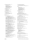
MB, 21264/EV68A command, 4–13, 4–21
MB_CNT Cbox CSR, operation
, 2–32
MBDone, SysDc command
, 4–13
Mbox
Dcache control register DC_CTL
, 5–30
Dcache status register DC_STAT
, 5–31
described
, 2–12
Dstream translation buffer
, 2–13
DTB address space number registers 0 and 1
DTB_ASNx
, 5–28
DTB alternate processor mode register
DTB_ALTMODE
, 5–26
DTB invalidate-all (ASM=0) process register
DTB_IAP
, 5–27
DTB invalidate-all process register DTB_IA,
5–27
DTB invalidate-single registers 0 and 1
DTB_ISx
, 5–27
DTB PTE array write registers 0 and 1
DTB_PTEx
, 5–26
DTB tag array write registers 0 and 1
DTB_TAGx
, 5–25
internal processor registers
, 5–2
load queue, 2–13
Mbox control register M_CTL
, 5–29
memory management status register
MM_STAT
, 5–28
miss address file
, 2–13
order traps
, 2–31
pipeline abort delay with order trap
, 2–16
pipeline abort delays
, 2–16
store queue
, 2–13
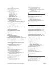
MBOX_BC_PRB_STALL Cbox CSR, defined
,
5–35
MCHK interrupt
, 6–14
Mechanical specifications
, 3–17
Memory
error case summary for
, 8–11
filling Dcache errors
, 8–8
filling Icache errors
, 8–7
Memory address space
load instructions with
, 2–27
merging rules
, 2–30
store instructions with
, 2–28
Memory barrier instructions
translation to external interface
, 4–5
Memory barriers
, 2–32
Memory reference unit. See Mbox
MF_FPCR instruction
, 6–12
Microarchitecture
summarized
, 2–1
MiscVref signal pin
, 3–5
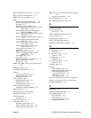
Miss address file
, 2–13
I/O address space loads
, 2–27
memory address space loads
, 2–27
memory address space stores
, 2–28
MM_STAT memory management status register
,
5–28
at power-on reset state
, 7–16
MT_FPCR instruction
, 6–12
MT_FPCR synchronous trap
, 6–14
N
NoConnect pin type, 3–3
Nonexistent memory
processing
, 4–38
NOP, 21264/EV68A command
, 4–21
Note convention
, xxi
Numbering convention
, xxi
NXM. See Nonexistent memory
NZNOP, 21264/EV68A command
, 4–21
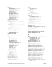
O
O_OD pin type, 3–3, 9–2
values for
, 9–4
O_OD_TP pin type
, 3–3, 9–2
values for
, 9–4
O_PP pin type
, 3–3, 9–2
values for
, 9–5
O_PP_CLK pin type
, 3–3, 9–2
values for
, 9–5
OPCDEC fault
, 6–13
Opcodes
IEEE floating-point
, A–9
independent floating-point
, A–11
reserved for Compaq
, A–8
reserved for PALcode
, A–9
summary of
, A–12
VAX floating-point
, A–11
Open-drain driver for test pins. See O_OD_TP
Open-drain output driver. See O_OD pin type
Operating temperature
, 10–1
P
Packaging, 3–18
Paired instruction fetch order
, 6–9
PAL_BASE register
, 5–15
after fault reset
, 7–8
after warm reset, 7–11
at power-on reset state
, 7–15
through sleep mode
, 7–10


