Two Port 10/100 Managed Ethernet Switch with 16-Bit Non-PCI CPU Interface
Datasheet
Revision 1.4 (08-19-08) 112 SMSC LAN9311/LAN9311i
DATASHEET
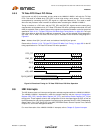
8.5.9 TX Data FIFO Direct PIO Writes
In this mode only A[2:1] are decoded, and any write to the LAN9311/LAN9311i will write the TX Data
FIFO. This mode is enabled when FIFO_SEL is driven high during a write access. This is normally
accomplished by connecting the FIFO_SEL signal to a high-order address line. This mode is useful
when the host processor must increment its address when accessing the LAN9311/LAN9311i.
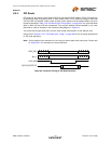
Timing is identical to a PIO write, and the FIFO_SEL and END_SEL signals have the same timing
characteristics as the address lines. A TX Data FIFO direct PIO write cycle begins when both nCS and
nWR are asserted. Either or both of these control signals must de-assert between cycles for the period
specified in Table 15.13, “TX Data FIFO Direct PIO Write Cycle Timing Values,” on page 453. The cycle
ends when either or both nCS and nWR are de-asserted. They may be asserted and de-asserted in
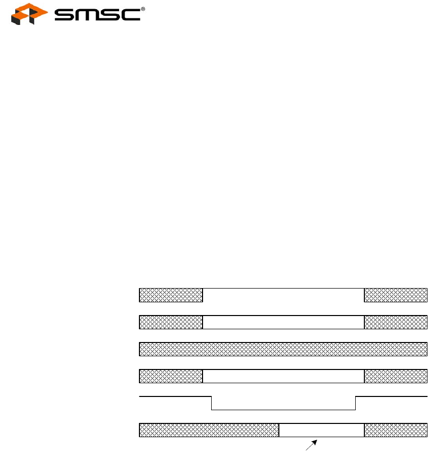
any order. The TX Data FIFO direct PIO write cycle is illustrated in the functional timing diagram in
Figure 8.8.
Note: Address lines A[2:1] are still used, and address lines A[9:3] are ignored.
Please refer to Section 15.5.9, "TX Data FIFO Direct PIO Write Cycle Timing," on page 453 for the AC
timing specifications for TX Data FIFO direct PIO write operations.
8.6 HBI Interrupts
The HBI allows access to all interrupt configuration and status registers within the LAN9311/LAN9311i.
The LAN9311/LAN9311i implements a multi-tier interrupt hierarchy with the Interrupt Configuration
Register (IRQ_CFG), Interrupt Status Register (INT_STS), and Interrupt Enable Register (INT_EN) at
the top level. These registers allow for the configuration of which interrupts trigger the IRQ, as well as
the IRQ deassertion and polarity properties. Interrupts may be generated from the 1588 Timestamping,
Switch Fabric, Port 1 PHY, Port 2 PHY, Host MAC, EEPROM Loader, General Purpose Timer, General
Purpose I/O, and Power Management blocks.
For more information of the LAN9311/LAN9311i interrupts, refer to Chapter 5, System Interrupts.
Figure 8.8 Functional Timing for TX Data FIFO Direct PIO Write Operation
VALID
D[15:0] (INPUT)
nCS, nWR
A[x:3]
VALID
END_SEL
VALID
A[2:1]
FIFO_SEL
(WRITE DATA TO TX DATA FIFO)


