142 AMD Geode™ SC3200 Processor Data Book
Core Logic Module
32581C
6.2.2.1 Video Retrace Interrupt
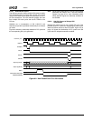
Bit 7 of the “Serial Packet” can be used to generate an SMI
whenever a video retrace occurs within the GX1 module.
This function is normally not used for power management
but for SoftVGA routines. Setting F0 Index 83h[2] = 1
enables this function. A read only status register located at
F1BAR0+I/O Offset 00h[5] can be read to see if the SMI
was caused by a video retrace event.
6.2.3 IDE Controller
The Core Logic module integrates a PCI bus mastering,
ATA-4 compatible IDE controller. This controller supports
UltraDMA, Multiword DMA and Programmed I/O (PIO)
modes. Two devices are supported on the IDE controller.
The data-transfer speed for each device can be indepen-
dently programmed. This allows high-speed IDE peripher-
als to coexist on the same channel as lower speed devices.
The Core Logic module supports two IDE channels, a pri-
mary channel and a secondary channel.
The IDE interface provides a variety of features to optimize
system performance, including 32-bit disk access, post
write buffers, bus master, Multiword DMA, look-ahead read
buffer, and prefetch mechanism for each channel respec-
tively.
The IDE interface timing is completely programmable. Tim-
ing control covers the command active and recover pulse
widths, and command block register accesses. The IDE
data-transfer speed for each device on each channel can
be independently programmed allowing high-speed IDE
peripherals to coexist on the same channel as older, com-
patible devices.
The Core Logic module also provides a software accessi-
ble buffered reset signal to the IDE drive, F0 Index 44h[2].
The IDE_RST# signal can be driven low or high as needed
for device-power-off conditions. IDE_RST# is not driven
low by POR# (Power-On Reset).
6.2.3.1 IDE Configuration Registers
Registers for configuring Channels 0 and 1 are located in
the PCI register space designated as Function 2 (F2 Index
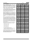
40h-5Ch). Table 6-35 on page 255 provides the bit formats
for these registers. The IDE bus master configuration regis-
ters are accessed via F2 Index 20h which is Base Address
Register 4 in Function 2 (F2BAR4). See Table 6-36 on
page 259 for register/bit formats.
The following subsections discuss Core Logic operational/
programming details concerning PIO, Bus Master, and
UltraDMA/33 modes.
6.2.3.2 PIO Mode
The IDE data port transaction latency consists of address
latency, asserted latency and recovery latency. Address
latency occurs when a PCI master cycle targeting the IDE
data port is decoded, and the IDE_ADDR[2:0] and
IDE_CS# lines are not set up. Address latency provides the
setup time for the IDE_ADDR[2:0] and IDE_CS# lines prior
to I
DE_IOR# and IDE_IOW#.
Asserted latency consists of the I/O command strobe
assertion length and recovery time. Recovery time is pro-
vided so that transactions may occur back-to-back on the
IDE interface without violating minimum cycle periods for
the IDE interface.
If IDE_IORDY is asserted when the initial sample point is
reached, no wait states are added to the command strobe
assertion length. If IDE_IORDY is negated when the initial
sample point is reached, additional wait states are added.
Recovery latency occurs after the IDE data port transac-
tions have completed. It provides hold time on the
IDE_ADDR[2:0] and IDE_CS# lines with respect to the
read and write strobes (IDE_IOR# and IDE_IOW#).
The PIO portion of the IDE registers is enabled through:
• Channel 0 Drive 0 Programmed I/O Register
(F2 Index 40h)
• Channel 0 Drive 1 Programmed I/O Register
(F2 Index 48h)
• Channel 1 Drive 0 Programmed I/O Register
(F2 Index 50h)
• Channel 1 Drive 1 Programmed I/O Register
(F2 Index 58h)
The IDE channels and devices can be individually pro-
grammed to select the proper address setup time, asserted
time, and recovery time.
The bit formats for these registers are shown in Table 6-35
on page 255. Note that there are different bit formats for
each of the PIO programming registers depending on the
operating format selected: Format 0 or Format 1:
• F2 Index 44h[31] (Channel 0 Drive 0 — DMA Control
Register) sets the format of the PIO register.
— If bit 31 = 0, Format 0 is used and it selects the
slowest PIO mode (bits [19:16]) per channel for
commands.
— If bit 31 = 1, Format 1 is used and it allows indepen-
dent control of command and data.
Also listed in the bit formats are recommended values for
the different PIO modes. Note that these are only recom-
mended settings and are not 100% tested.
When using independent control of command and data
cycles the following algorithm should be used when two
IDE devices are sharing the same channel:
1) The PIO data cycle timing for a particular device can
be the timing value for the maximum PIO mode which
that device reports it supports.
2) The PIO command cycle timing for a particular device
must be the timing value for the lowest PIO mode for
both devices on the channel.


