AMD Geode™ SC3200 Processor Data Book 217
Core Logic Module - Bridge, GPIO, and LPC Registers - Function 0
32581C
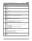
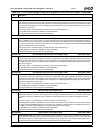
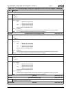
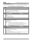
Index CCh User Defined Device 1 Control Register (R/W) Reset Value: 00h
7 Memory or I/O Mapped. Determines how User Defined Device 1 is mapped.
0: I/O.
1: Memory.
6:0 Mask.
If bit 7 = 0 (I/O):
Bit 6 0: Disable write cycle tracking
1: Enable write cycle tracking
Bit 5 0: Disable read cycle tracking
1: Enable read cycle tracking
Bits [4:0] Mask for address bits A[4:0]
If bit 7 = 1 (Memory):
Bits [6:0] Mask for address memory bits A[15:9] (512 bytes min. and 64 KB max.) A[8:0] are ignored.
Note: A "1" in a mask bit means that the address bit is ignored for comparison.
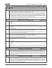
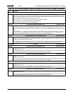
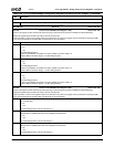
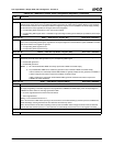
Index CDh User Defined Device 2 Control Register (R/W) Reset Value: 00h
7 Memory or I/O Mapped. determines how User Defined Device 2 is mapped.
0: I/O
1: Memory
6:0 Mask.
If bit 7 = 0 (I/O):
Bit 6 0: Disable write cycle tracking
1: Enable write cycle tracking
Bit 5 0: Disable read cycle tracking
1: Enable read cycle tracking
Bits [4:0] Mask for address bits A[4:0]
If bit 7 = 1 (Memory):
Bits [6:0] Mask for address memory bits A[15:9] (512 bytes min. and 64 KB max.) A[8:0] are ignored.
Note: A "1" in a mask bit means that the address bit is ignored for comparison.
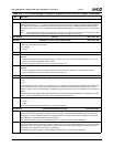
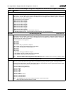
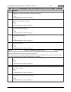
Index CEh User Defined Device 3 Control Register (R/W) Reset Value: 00h
7 Memory or I/O Mapped. Determines how User Defined Device 3 is mapped.
0: I/O.
1: Memory.
6:0 Mask.
If bit 7 = 0 (I/O):
Bit 6 0: Disable write cycle tracking
1: Enable write cycle tracking
Bit 5 0: Disable read cycle tracking
1: Enable read cycle tracking
Bits [4:0] Mask for address bits A[4:0]
If bit 7 = 1 (Memory):
Bits [6:0] Mask for address memory bits A[15:9] (512 bytes min. and 64 KB max.) A[8:0] are ignored.
Note: A "1" in a mask bit means that the address bit is ignored for comparison.
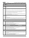
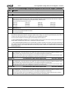
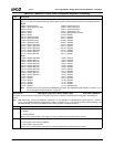
Index CFh Reserved Reset Value: 00h
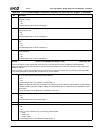
Index D0h Software SMI Register (WO) Reset Value: 00h
7:0 Software SMI. A write to this location generates an SMI. The data written is irrelevant. This register allows software entry
into SMM via normal bus access instructions.
Index D1h-EBh Reserved Reset Value: 00h
Table 6-29. F0: PCI Header/Bridge Configuration Registers for GPIO and LPC Support (Continued)
Bit Description


