204 AMD Geode™ SC3200 Processor Data Book
Core Logic Module - Bridge, GPIO, and LPC Registers - Function 0
32581C
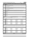
1 Floppy Disk Access Trap.
0: Disable.
1: Enable.
If this bit is enabled and an access occurs in the address ranges listed below, an SMI is generated.
— Primary floppy disk: I/O Port 3F2h-3F5h, 3F7h.
— Secondary floppy disk: I/O Port 372h-375h, 377h.
Top level SMI status is reported at F1BAR0+I/O Offset 00h/02h[0].
Second level SMI status is reported at F0 Index 86h/F6h[1].
0 Primary Hard Disk Access Trap.
0: Disable.
1: Enable.
If this bit is enabled and an access occurs in the address ranges selected in F0 Index 93h[5], an SMI is generated.
Top level SMI status is reported at F1BAR0+I/O Offset 00h/02h[0].
Second level SMI status is reported at F0 Index 86h/F6h[0].
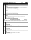
Index 83h Power Management Enable Register 4 (R/W) Reset Value: 00h
7 Secondary Hard Disk Idle Timer Enable. Turn on Secondary Hard Disk Idle Timer Count Register (F0 Index ACh) and
generate an SMI when the timer expires.
0: Disable.
1: Enable.
If an access occurs in the address ranges selected in F0 Index 93h[4], the timer is reloaded with the programmed count.
Top level SMI status is reported at F1BAR0+I/O Offset 00h/02h[0].
Second level SMI status is reported at F0 Index 86h/F6h[4].
6 Secondary Hard Disk Access Trap. If this bit is enabled and an access occurs in the address ranges selected in F0 Index
93h[4], an SMI is generated.
0: Disable.
1: Enable.
Top level SMI status is reported at F1BAR0+I/O Offset 00h/02h[0].
Second level SMI status is reported at F0 Index 86h/F6h[5].
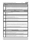
5 ACPI Timer SMI. Allow SMI generation for MSB toggles on the ACPI Timer (F1BAR0+I/O Offset 1Ch or
F1BAR1+I/O Offset 1Ch).
0: Disable.
1: Enable.
Top level SMI status is reported at F1BAR0+I/O Offset 00h/02h[0].
Second level SMI status is reported at F0 Index 87h/F7h[0].
4 THRM# SMI. Allow SMI generation on assertion of THRM#.
0: Disable.
1: Enable.
Top level SMI status is reported at F1BAR0+I/O Offset 00h/02h[0].
Second level SMI status is reported at F0 Index 87h/F7h[6].
3 VGA Timer Enable. Turn on VGA Timer Count Register (F0 Index 8Eh) and generate an SMI when the timer reaches 0.
0: Disable.
1: Enable.
If an access occurs in the programmed address range, the timer is reloaded with the programmed count. F0 Index 8Bh[6]
selects the timebase for the VGA Timer.
SMI status is reported at F1BAR0+I/O Offset 00h/02h[6] (top level only).
Table 6-29. F0: PCI Header/Bridge Configuration Registers for GPIO and LPC Support (Continued)
Bit Description


